ASRock has a history of bringing new features to motherboards where others can tread conservatively. In recent generations, this means the Extreme11 range with an onboard LSI3008 for SATA ports, or the C2750D4I, an octo-core Atom platform with 64GB DRAM support and 12 SATA ports on a mini-ITX. For the ASRock Z97 Extreme6 we have an M.2 slot that runs at PCIe x4, with lanes taken direct from the CPU. We test the motherboard, the performance of this slot, and the effect of dual-GPU gaming with four CPU PCIe lanes tied up in storage.
ASRock Z97 Extreme6 Overview
The big feature point of the Z97 Extreme6 is the Ultra M.2 port, offering PCIe 3.0 x4 bandwidth direct from the CPU. This technically suggests a theoretical maximum bandwidth of 32 Gbps / 4 GBps, or 3.938 GBps with the 128/130b encoding afforded by PCIe 3.0. Using regular interpolation of storage overhead, this would mean a peak read/write of 3.2 GBps should the drive be sufficient. ASRock was kind to pass on one of the few native PCIe 3.0 x4 drives in OEM circulation, the Samsung XP941 (read Kristian’s review here). Using this drive we saw a peak read speed on IOmeter of 1.35 GBps, far from the peak that the slot can handle, but it does certainly give plenty of headroom for future devices and earmarks an important development in NGFF devices. The Z97 Extreme6 also has an M.2 x2 slot from the chipset PCIe 2.0 lanes, on which the same drive achieves a 828 MBps peak sequential.
In order to equip the motherboard with an M.2 x4 port, ASRock had two choices. They could combine four lanes from the chipset/PCH into a single slot, although that would severely limit the number of controllers that could be placed on the motherboard without additional PCIe switches. The other method was in the x8/x4/x4 allocation from the CPU, earmarking the final x4 for the M.2. In this method, installing an M.2 drive in this x4 slot would reduce any chipset overhead, but it would also reduce the other PCIe lanes down to x8/x4. This removes any chance of SLI, but Crossfire can still be used in x8/x4. As part of this review, we tested two 7970s at x8/x4 while the XP941 was installed and saw less than a 1% drop in frame rates for our game tests. This is highly important for a few reasons. It means that any motherboard manufacturer should be able to implement this without impacting the frame rates in reviewer benchmarks. It might also drive NVIDIA to remove the x8 lane restriction on SLI so that users can enjoy dual NVIDIA gaming while using an M.2 drive. It also means that Intel needs to step up the number of PCIe lanes on the mainstream CPUs, to at least 20 if not more. This would allow x8/x8 SLI + x4 for M.2, or x8/x4 with two x4 M.2 slots, or any kind of crazy combination therein. Despite the lack of commercial M.2 x4 drives on the market, the fact that ASRock has pursued this whereas the other major motherboard manufacturers did not should land kudos on ASRock’s shoulders.
That all being said, the Z97 Extreme6 falls afoul of some of the same routing issues we encountered with Z97-Deluxe. The SATA Express connector shares bandwidth with the two SATA ports associated with it, which is not that odd, but it also shares bandwidth with the M.2 x2 slot. To combat this, ASRock has another 8 SATA 6 Gbps ports, but one of these is shared with the eSATA port on the rear. That leaves seven SATA ports if the rest were used, but making sure the right ones are being used first time requires double checking.
The ASRock Z97 Extreme6 uses a series of hubs and controllers to provide all the ports on board. The USB 3.0 ports are split such that the two headers are from the chipset, four of the rear ports are from an ASM1074 hub, and the final two from an ASM1042e controller to give 10 USB 3.0 in total. There is an ASMedia PCIe Gen 2.0 switch as well, the ASM1184, which use one upstream port for four downstream ports. ASRock has split these ports to provide two of the PCIe 2.0x 1 slots (one of which uses a quick switch to the mini-PCIe) and the four SATA 6 Gbps from ASM1061 controllers.
Aside from the PCIe allocation, the Z97 Extreme6 retains the onboard vertical USB 2.0 port from their high-end Z87 products and implements twin BIOS functionality. Out of the six fan headers on-board, only one is four pin, and the extra power for the PCIe devices comes from a 4-pin molex. Like most other manufacturers, ASRock implements this motherboard with an enhanced Realtek ALC1150 audio system, involving PCB separation, filter capacitors and headphone amplification, dubbed Purity Sound 2. The two network interfaces on board come from the Intel I218-V and a Realtek 8111GR.
On the performance side, the ASRock Z97 Extreme6 smashes the DPC Latency record from our last review, bringing the best latency down to a 39 microsecond peak. While the Windows 7 POST time is poor (almost 20 seconds), when controllers are disabled this time drops to seven seconds only. Power consumption during load was 10-20W higher than some of the other Z97 motherboards we have tested, but the rest of the benchmarks were on the same level. The automatic overclocking options are plentiful from the BIOS and a few to the OS, and manual overclocking gave our i7-4770K CPU a good 4.6 GHz at 1.300 volts before temperatures became the main concern.
The Extreme6 is the cheapest Z97 motherboard we have tested so far, at $ 170, and is the only motherboard currently on sale with an integrated M.2 x4 slot (the Extreme9 will have one, but is not available yet). So while this offers a good opportunity for ASRock to flex its engineering muscles, the lack of PCIe M.2 drives (either x2 or x4) currently on the market is the biggest drawback.
Visual Inspection
Back in our pre-release Z97 motherboard article, I noted how ASRock’s color scheme for their motherboard range has transformed into something more vibrant than before. Unlike other manufacturers which are blending darker or dulled colors, ASRock is hitting the saturation on full. The overclocking range ‘OC Formula’ is a strong mustard yellow, the gaming ‘Fatal1ty’ range is a vibrant red and the channel ‘extreme’ range is the big blue we see below.
The socket area pushes the chokes outside the Intel specifications, giving slightly more room for larger air coolers. But the DRAM slots are right up against that specification, and as such there might be issues with tall memory modules and large coolers. The socket area has access to four of the six fan headers on board – two CPU headers between the top heatsink and the memory slots, 3-pin PWR header at the top right of the motherboard and a 3-pin CHA header next to the motherboard CR2032 battery. Because this motherboard only has a single 4-pin header, it is perhaps wise to have placed it near the socket, however we should push ASRock to implement a full complement of 4-pin headers.
The DRAM slots next to the socket seem like the slightly thinner versions that are often seen on the cheaper motherboard lines, however they did work fine in our testing. These slots use double-ended latch mechanisms as well.
On the right hand side of the motherboard we have one of the chipset USB 3.0 headers underneath the 24-pin ATX power connector, followed by the mélange of SATA 6 Gbps ports. Despite them all being the same color, the top four ports are the ones from the ASMedia 1061 controllers (via the ASM1184, so they all have the same upstream bandwidth shared with two of the PCIe 2.0 x1 slots) and the bottom six are from the chipset.
The SATA Express port requires specific spacing between the SATA ports and as such we can see two of the plastic moldings for them bonded together on the motherboard. This is a different application of SATA Express compared to the other motherboards we have reviewed which all use a single combination connector for all concerned. I wonder if that is several cents more expensive than the layout ASRock has managed here. Nevertheless it is worth noting that the SATA Express shares bandwidth with the M.2 x2 slot, meaning that any SATA device connected to SATAe disables M.2 and vice versa. To ensure that a specific device is recognized, it is advised to manually adjust the option in the BIOS.
On the bottom right of the board are two removable BIOS chips, a 3-pin fan header, a BIOS selection switch, the power and reset buttons, a two-digit debug, the front panel header, a vertical USB 2.0 and a new feature, the HDD Saver header. HDD Saver is one of those ASRock-specific features new for 9-series, whereby a user can hook up two SATA devices via this header and the included cable and have immediate control of the power of those devices in the OS. In this way a user can disable, in software, their ODD/HDDs in order to save data from outside interference (for example, backups) or save power.
Elsewhere on the rear panel are USB 2.0 headers, the second chipset USB 3.0 header, a Thunderbolt Add-In-Card header, a 3-pin fan header, a COM header and the 4-pin molex power for the PCIe slots. Although I have mentioned this on many other reviews, when it comes to PCIe power, the 4-pin molex connector is a bad connector due to size and the limited use they now have in most PC builds. Most manufacturers have moved onto either SATA power or a 6-pin PCIe for power, but ASRock still insist on a 4-pin molex connection.
The Purity Sound 2 audio subsystem uses a separated PCB and an EMI shield around the Realtek ALC1150 codec. Filter caps and headphone amplifiers are also used.
The rear panel forgoes any USB 2.0 implementation, even though I believe ASRock could have purchased the appropriate connectors to get all the features they wanted in. From left to right is a combination PS/2 port, two USB 3.0 from the ASM1074 hub, a DVI-I, a ClearCMOS button, an eSATA 6 Gbps, DisplayPort, HDMI, an Intel I218-V NIC, two more USB 3.0 from the ASM1074 hub, two USB 3.0 from an ASM1042AE controller, a Realtek 8111GTR NIC and the audio jacks on the end.
Four DDR3 DIMM slots supporting up to 32 GB Up to Dual Channel, 1333-3200 MHz
Video Outputs
HDMI (4096×2304 at 24 Hz) DVI-I (1920×1200 at 60 Hz) DisplayPort 1.2 (4096×2304 at 24 Hz or 3840×2160 at 60 Hz)
Onboard LAN
Intel I218-V Realtek RTL8111GR
Onboard Audio
Realtek ALC1150
Expansion Slots
2 x PCIe 3.0 x16 (x16 or x8/x8) 1 x PCIe 2.0 x4 (x2 only) 2 x PCIe 2.0 x1 1 x mini-PCIe (shares bandwidth with PCIE3, an x1 slot)
Onboard SATA/RAID
6 x SATA 6 Gbps (PCH), RAID 0, 1, 5, 10 4 x SATA 6 Gbps (ASM1061) (SATA3_A4 shared with eSATA) 1 x SATA Express (shared with SATA3_4, SATA3_5 and M2_2) 1 x eSATA 6 Gbps (ASM 1061) (Shared with SATA3_A4) 1 x Ultra M.2 x4 (CPU) 1 x M.2 x2 (shared with SATAe, SATA3_4, SATA3_5)
USB 3.0
4 x USB 3.0 (PCH) [2 headers] 2 x USB 3.0 (ASM1042A controller) [2 rear panel] 4 x USB 3.0 (ASM1074 hub) [4 rear panel]
Onboard
10 x SATA 6 Gbps 1 x SATAe 1 x M.2 x4 1 x M.2 x2 2 x USB 3.0 Headers 2 x USB 2.0 Headers 1 x TPM Header 6 x Fan Headers 1 x HDD Saver Header 1 x Thunderbolt AIC Connector 1 x USB 2.0 Vertical Type A 1 x Two-Digit Debig Power/Reset Swtiches BIOS Selection Switch Front Audio Header Front Panel Header
Power Connectors
1 x 24-pin ATX 1 x 8-pin CPU 1 x 4-pin Molex (for VGA)
Fan Headers
2 x CPU (4-pin, 3-pin) 3 x CHA (3-pin) 1 x PWR (3-pin)
IO Panel
1 x Combination PS/2 1 x Clear_CMOS Button 1 x eSATA 6 Gbps DVI-I DisplayPort HDMI 2 x USB 3.0 (ASM1042AE) on far right 4 x USB 3.0 (ASM1074 hub) Intel I218-V gigabit Ethernet on left Realtek RTL8111GTR gigabit Ethernet on right Audio Jacks
As mentioned in my previous Z97 reviews, with the demands on PCIe lanes from the chipset being stretched thinner with the new M.2 and SATAe requirements, I predicted we would be seeing more USB 3.0 hubs in use to ease that burden. The big plus in ASRock’s favor is the PCIe 3.0 x4 M.2 port, which can be used in 2-way Crossfire. Unfortunately due to NVIDIA restrictions, the x4 M.2 cannot be used with SLI, but the x2 M.2 can be. I could imagine ASRock placing two of these x4 M.2 slots onto the rear of a mini-ITX motherboard, and giving the main PCIe slot only x8 lanes (our tests later in the review show our gaming results with little difference between PCIe 3.0 x8 and x16).
With every new chipset release, a large part of the community is always interested in the smaller form factor builds. Building a small yet powerful system seems to be an expanding niche, and for Intel’s Z97 platform we took three of the cheaper mini-ITX motherboards to see how they compare. The ASRock Z97E-ITX/AC, the MSI Z97I AC and the GIGABYTE Z97N-WIFI are all between $ 130 and $ 140, all feature 802.11ac support but vary in other connectivity, ease of use and their packages. We compared all three.
Z97 Mini-ITX Overview
What does the average user want from a mini-ITX system? Is there such a thing as an average user, or are all mini-ITX builds aimed at niche categories? Even these questions can be difficult to pin down, so we have to look at the basics for a 17cm square focal point.
Mini-ITX builds are typically not the center for overclocking, although they should be designed to house the most powerful processors (at least at stock). Two memory slots limits the memory capacity to 16 GB, which for VM use limits anything other than a simple virtualization environment with a handful of instances. The PCIe 3.0 x16 slot is usually a big plus, allowing gamers to equip the best single GPU card into a small system, or for home NAS builds to implement a RAID card, or for TV Tuner/HTPC applications. To date, I have built four mini-ITX systems for friends and family. My father uses one on the integrated graphics for a home/email/basic photo and video editing machine, while my brother has a nice discrete GPU for gaming on a single monitor. I own the other two, one on basic HTPC/streaming duty and the other as part of a makeshift NAS. Each of these four systems uses a different motherboard for requirements: the basic home-use machine uses an mSATA drive, the NAS has dual NICs, the HTPC has 2T2R 802.11ac WiFi and the gaming system has pretty lights for the see-through panel.
With the $ 130-$ 140 motherboards we are testing today, we could try and fit them into these four categories based on their hardware, functionality and performance. Being very close in price means that one motherboard will swap in a feature at the expense of another, so one would expect a lot of tit-for-tat between the manufacturers. Of course, anything in the box or on the software side could sweeten the deal, but it all depends if they end up being focused on one niche or a jack-of-all-trades.
ASRock Z97E-ITX/AC Visual Inspection
The first motherboard on the test bed was the ASRock Z97E-ITX/AC. In the past couple of generations, ASRock has done something slightly different to the others and it appears again on the Z97 model: a storage option on the rear of the motherboard. Usually when I mention this to people, the answer comes back ‘does this not touch the case?’ My answer comes back as ‘depends how big your stand-offs are’. The Z77 model with an mSATA equipped has no problems in a Bitfenix Prodigy, for example. Where the Z97E-ITX/AC differs for this generation is the switch from mSATA to M.2 on the rear.
The M.2 on the rear is only applicable for 30mm and 42mm, which is actually rather short, due to the orientation. As this is a PCIe and SATA capable M.2, this opens up the drive potential, however I feel the migration of the majority of motherboards to 80+mm drives might make the lower dimension models harder to find (as well as in lower capacities), making ASRock’s solution niche in more ways than one.
The primary design route of the Z97E-ITX/AC is similar to that of the predecessors. We get a top oriented socket to allow for larger coolers north to south, although the left to right spacing of the socket might obstruct the combination of large CPU heatsink and large DRAM heatsinks. The 6-phase power delivery has the ASRock styled heatsink, and the two fan headers are found at opposite ends of the socket – one top left and the other bottom right.
My first two issues with this board related to the number of fan headers (premium motherboards are getting three, even if two are connected together), and the second is with the 8-pin CPU power connector placement. One of the more prominent issues I have echoed with mini-ITX design is this placement, which (in my opinion) should be anywhere BUT the middle of the motherboard near the rear-IO. This is one of the worst places, because the cable to put in that port has to either navigate around a CPU heatsink, come across the DRAM and around a CPU heatsink or navigate over a PCIe device. Other motherboard manufacturers have recognized this, and oriented their power connectors nearer the edges of the board, but ASRock is still behind. I will not accept ‘ease of routing’ as an excuse here, especially if the engineers are putting M.2 slots on the rear of the motherboard.
The DRAM slots use a single sided latch mechanism on the bottom of the board so as to not interfere with any GPU, although users should ensure that all the memory is fitted properly. On the top right of the board is the motherboard battery, set up in this location and standing up on the motherboard in order to save space. The 24-pin power connector is underneath, followed by the USB 3.0 header, front panel header and TPM header.
The location of the SATA ports between the DRAM and the mini-PCIe module is such that we get four SATA 6 Gbps in grey, two SATA 6 Gbps in black, and these last two ports form part of a SATA Express connector. One of the issues with this arrangement is the removal of devices with locking cables, requiring the user to disconnect other cables, or due to the location also requiring the DRAM or the GPU to be moved in order to get a hand in.
It should be noted that the SATAe connector, the two SATA 6 Gbps ports in black and the M.2 slot on the rear are all on a switch, thus using one will disable the other two. Unfortunately this is a limitation of the Intel chipset, and the lack of drives on the market for either of the PCIe storage options does not make the selection easier.
The mini-PCIe connector holds the included 802.11ac 2T2R WiFi module, and the two antenna points on the module are connected to the rear IO via internal wires. This is next to the chipset with a small heatsink, two USB 2.0 ports and the front panel audio port. The ASRock mini-ITX motherboard is a little different to the other two as the audio codec used is the better rated Realtek ALC1150 rather than the ALC892.
The rear panel gives a combination PS/2 port, two USB 2.0 ports, the combination DVI-I port, two antenna mounting points, both a HDMI-In and a HDMI-Out (for pass-through), DisplayPort 1.2, a ClearCMOS button, four USB 3.0 ports, the Intel I218-V gigabit Ethernet port and the audio jacks.
MSI Z97I AC Visual Inspection
The first thing that immediately jumps out at me on the MSI Z97I AC is the position of the 4-pin CPU power connector. We find it just behind the rear panel, in the middle of the motherboard and slightly to the left. I have rallied for several generations now that this is perhaps the worst place to have this power connector. Any cable coming into this connector has to either jump over the SATA ports and front panel ports, jump over the DRAM then around the CPU heatsink, or jump over the graphics card. All three of these possibilities cause nightmares for cable management, and I would like this position to stop – now.
So the argument for having this power connector here is because the CPU socket is lower down on the motherboard, allowing the connectors related to the chipset space at the top. The second reason is one of cost – moving the DRAM inwards and placing connectors on the outside requires more PCB layers, and moving from a four layer to a six layer adds 30-50% cost to the PCB, depending on the quality of PCB used. At some point we are going to have to reach a happy medium: I believe there is a solution to a $ 130 motherboard having the connectors in decent places and the motherboard still retaining on the functionality.
Ranting aside, the CPU socket is up against the DRAM slots and near the PCIe connector, which might limit the size of the heatsink if tall memory or a large GPU is used. The power delivery uses a four phase solution with a heatsink, with the CR2032 battery at right angles underneath. The two DRAM slots are on the right hand side and use a single sided latch mechanism.
All the main headers and connectors are at the top of the motherboard, starting with the mini-PCIe on the right hand side with the Intel 802.11ac AC7260 2T2R solution. The antennas are connected to the rear panel with a wire, which might get in the way of some of the other headers if the user is not careful. Between the WiFi module and the chipset are the COM header and the CPU 4-pin header. The other fan header is just above the power delivery heatsink.
At the top left of the motherboard are four SATA 6 Gbps ports, next to the USB 3.0 header. Below this are a USB header and the front panel headers. It is worth noting that the front panel header has no indication or color coordination letting the user know which cable goes where, which I feel is a missed opportunity to improve user experience. The audio codec and filter caps are at the bottom left of the motherboard, next to the PCIe 3.0 x16 slot.
The rear panel makes room for the antennas and dual Realtek NICs, but also the addition of two buttons on the left. One of them is for ClearCMOS and the other for Go2BIOS. The rear panel also has four of the chipset USB 3.0 ports, two USB 2.0 ports, a combination PS/2 port, three video outputs and audio jacks.
Unlike the ASRock motherboard, it is worth noting that there are no PCIe storage options on the MSI.
GIGABYTE Z97N-WIFI Visual Inspection
The immediate visual cues that separate the GIGABYTE Z97N-WIFI from the other two motherboards in this review is firstly the lack of a power delivery heatsink, and then the position of almost all the motherboard connectors around the outside of the PCB, including the 4-pin CPU power delivery.
In the past, I criticized GIGABYTE for their component placement, but it would seem that the Z97N-WIFI gets a near perfect score. Along the top are the 4-pin CPU power connector, the COM header and the two fan headers, while on the right hand side (note, on the edge of the PCB) is the 24-pin ATX power connector, two of the SATA ports, the front panel header, a USB 2.0 header and a USB 3.0 header. Actually the only ports slightly away from the edge are the other four SATA ports, but given that two are on the outside that makes building a PC a lot easier.
The lack of a power delivery heatsink might give cause for concern for overclocking, however GIGABYTE is claiming to use high efficiency power delivery ICs and our overclock testing differs little from the other two motherboards.
The mini-PCIe slot for the wireless module is near the rear panel which keeps the wires for the antenna very short and does not block any other headers on the motherboard. The two fan headers at the top of the motherboard might be a little localized, and perhaps another header on the right, or lower down the motherboard, might be well received.
The socket area is above the chipset for the GIGABYTE board, with the only barrier to large CPU coolers being tall DRAM modules, although with some regular or low profile modules it looks like this motherboard could cope with almost any large air cooler. To save space, GIGABYTE has stuck the motherboard battery to the rear panel, something we have seen in previous iterations.
The rear panel of the GIGABYTE motherboard affords another difference to the other motherboards – two HDMI-out ports. This is backed up with a DVI-I, but no DisplayPort here. The panel also includes a combination PS/2 port, two USB 2.0 ports, four USB 3.0 ports, an Intel I217-V NIC, an Atheros AR81 NIC and the audio jacks (Realtek ALC892).
Similarly to the MSI, there are no PCIe storage options here, and the audio codec matches that of the MSI.
Unlike other manufacturers, GIGABYTE puts a block diagram of each motherboard in their manuals. Here we can see where all the PCIe lanes end up being distributed. Due to the limited size of mini-ITX, only a few are used.
When we looked at AMD’s Kabini platform, AMD in its press materials pitted their high end APU against the Pentium J2900 in terms of price and performance. The only issue from the reviewer’s standpoint was the availability of the Pentium J2900 in a retail product. At the time, the J2900 was found only in OEM devices, or a single system was found through Google Shopping. Fast forward a few months and we are now seeing a small wave of J2900 motherboards coming to market for custom home builds. ASRock look poised to release the Q2900-ITX and Q2900M to meet that demand.
As both motherboards are using the quad core J2900 at 2.40 GHz (2.66 GHz turbo) and 10W, both are supplied with large fanless heatsinks to provide the cooling. The CPU is soldered on to the motherboard (this is an Intel limitation) meaning upgrading is not possible, but the CPU does offer dual channel DDR3, 2 MB of L2 cache and Intel HD graphics.
The Q2900-ITX is an ITX motherboard that relies on SO-DIMM DDR3 memory. The standard Atom chipset ports are here – two SATA 6 Gbps, two SATA 3 Gbps, four USB 3.0 ports, a PCIe 2.0 x1 slot, a mini-PCIe slot (for WiFi) and three standard video outputs (VGA, DVI-D, HDMI).
The Q2900M goes up to the micro-ATX size, which affords use of full-sized DDR3. Note how each of the DDR3 DIMMs are at right angles to each other, which comes across as really, really odd. The PCIe lane layout is a little different, giving a full sized PCIe slot capable of PCIe 2.0 x4. There is also two other PCIe 2.0 x1 slots, however judging by other motherboards of this ilk, using the PCIe 2.0 x4 will disable the other PCIe ports or vice versa.
While AMD’s FX-9590 CPU has been in systems for over a year, it suddenly comes to market as a retail package for end-users to buy with a bundled liquid cooling system. This 220W CPU that has a turbo speed of 5.0 GHz still sits at the top of AMD’s performance stack, despite subsequent improvements in the architecture since. We have decided to grab ASRock’s 990FX Extreme9 and an FX-9590 for a review to see if it still is the AMD performance CPU champion.
Spot the CPU
The story behind AMD’s fastest ever x86 CPUs is slightly odd. Two models, the FX-9590 and FX-9370, were both launched into OEM channels in June 2013. Being an OEM component, the only way to get one was in a pre-built system through a retailer, or through a bulk system integrator that had a model around one of these CPUs. Typically this is a process that is only exhibited with server class processors: from a range of CPUs being produced, only several will be available for end-users at retail because server CPUs usually go through a system builder. At the time, it seemed that AMD concerned that the high TDP of this CPU, at 220W listed, is too much for most cooling setups within a home user system and the best way to get it to consumers would be if a system builder chose the appropriate cooling for them.
As a result of this orientation of sales, AMD did not sample the media with review units. We review an AMD product typically though an AMD sourced sample. It was also noted that the OEM price for the CPU was near $ 900 for the FX-9590, which seemed like an excruciating amount for what was essentially a good overclocking version of the FX-8350. Several media websites were able to collaborate with system builders in order to get a chance to review the CPU, and AMD was confident in their promotion and handling of the new CPU.
Anecdotally, in my field of vision, the promotion of this CPU was relatively limited. The price was the main factor, resulting in comparative AMD/Intel systems being more power hungry on the AMD side, and substantially more expensive when put up against the latest mainstream i7 at the time. As a result, while some retailers were selling the OEM CPU at full price, some retailers decided to sell their OEM stock with a severe price cut directly to consumers, down from $ 900 to $ 390, in order to get rid of units (this is when I picked up our sample).
Due to the OEM nature of these sales to end-users, each CPU had either no warranty with AMD or a limited warranty. For the user interested in a 3-year system cycle without the fear of a bad egg, the OEM route is never a positive one.
AMD subsequently released, relatively silently, a proper package and retail version of the FX processors. It was apparent that this was in response to the OEM sales, with the retailers list ‘heatsink and fan not included’ alongside the specifications.
Since that release, AMD has not upgraded their enthusiast processor line with the latest architecture. The FX line has stayed where it is, perhaps for a number of reasons. One could speculate that releasing the next generation of FX-85xx might put them behind the FX-9590 in performance, or that the fabrication process was not suitable for a quad-module CPU with the new architecture improvements. The FX line for desktops, as far as we know, is staying at 32nm with no improvements.
Now Available
Fast forward twelve months to June 20th 2014 and Roy Taylor, AMD’s VP of Global Channel Sales tweets this innocuous picture:
Speculation was rife as to what this was. Here is a large box for an FX processor with the words ‘with Liquid Cooling System’ underneath. AMD supplied liquid cooling to the media when we reviewed the FX-8350 CPUs, the main CPU that sits underneath the FX-9590 and FX-9370, so there was an expectation that was something new.
On June 26th, the @AMDFX twitter account posted the following, confirming that this was the older FX-9590 but in a retail box with retail cooling:
The AMD FX Processor page has been updated accordingly, showing the same render of the new box. Here we see that the liquid cooler is supplied by Cooler Master, and uses a wide range PWM fan as part of the package.
Of course, this leaves several questions unanswered: how much, when is it on sale, where is it on sale, and is it still any good? Well for the US at least, it is on sale today from Newegg at $ 370 with the water cooling kit, or $ 330 without. NCIX has it listed for CAD$ 500, although this is currently in ‘back stock’ mode.
The SKU to look for is the FD9590FHHKWOX, which in the UK does not seem to be on the shelves as of yet. Amusingly, when this is typed in to Google, the search engine asked me if I meant FD9590FHHKWOF, the non-CLC version.
This Review
Back when the FX-9590 was originally released alongside the FX-9370, we were unable to secure a sample from AMD and the limited availability made us feel the CPU had a fairly limited scope for testing. However, now the landscape has changed. There has been no new FX CPUs on the market from AMD, and this subsequent release of a retail version piques the interest as to how relevant AMD still sees their high-frequency part. Because I now have a FX-9590 all of my own to test from when the OEM stock was sold, I felt it was worth revisiting to see if it can be considered an investment.
Alongside testing this CPU, the 220W TDP requires a substantial motherboard to match. Due to the age of the platform, the AM3+ socket and the old 990FX chipset, finding a motherboard can be rather tricky. Many of the AM3+ motherboards that were launched were only suited for the FX-8350 processors, which had a 125W TDP. This is yet another reason that AMD wanted the FX-9590 in the hands of system builders who would chose high end motherboards that could cope.
Two of the newest motherboards to be released for 990FX were the ASRock 990FX Killer and the ASRock 990FX Extreme9. We reported the release of the Killer in December 2013, but the Killer is unsuitable here as the specification sheet lists processors up to 125W only. The Extreme9 is ASRock’s high-end AM3+ motherboard, and more suited to the task. Luckily I had requested a sample almost a year ago for some regression testing, so we will be reviewing this motherboard as part of this article.
One of the problems of Intel’s high end desktop platforms is size: the sockets are large, and all the DRAM slots take up a fair amount of space. Couple this with the PCIe lane potential of the CPU, then restricting the motherboard size smaller than ATX limits the number of features and multi-PCIe capabilities afforded by the platform. Nonetheless we saw a couple of motherboards for X79 move down to the micro-ATX size, as well as a few system designer builds that offered other sizes. In that vein, ASRock is moving from its X79 Extreme4-M (our review) and sent us pictures of the upcoming X99M Killer.
One thing that a micro-ATX layout does is free up some of the PCIe lanes for extra controllers. The X99M Killer will have ASRock’s Ultra M.2, giving PCIe 3.0 x4 bandwidth for devices up to 22110. Being part of ASRock’s Killer range we get an E2200 series network interface, which also incorporates an EM shield similar to the Purity Sound 2 upgraded audio. The Killer NIC is paired with an Intel NIC as well, with the Fatal1ty Mouse Port also appearing.
Due to the size, if any other mATX motherboards are released I would assume that like the X99M Killer there will only be four DDR4 memory slots, and here ASRock have used thinner slots in order to fit the power delivery and other features on board. I count five fan headers on the board, along with ASRock’s HDD Saver connector and ten SATA 6 Gbps ports. I can just about make out that some of these are labelled SATA3_0_1 and some are labelled 5_SATA3_0_1, perhaps indicating the presence of a controller or a hub. There is also a USB 3.0 header on board with power/reset buttons, a two digit debug, two BIOS chips, two USB 2.0 headers, a COM header and additional power to the PCIe slots via s 4-pin molex. We also have an eSATA on the rear panel, with a ClearCMOS button.
We can make out the final PCIe slot as having only four lanes of pins, suggesting an x16/x16/x4 layout. Whether these four lanes are from the CPU or the chipset is unclear, especially with the presence of the PCIe 3.0 M.2 x4 slot in the middle.
The box lists XSplit, indicating a bundling deal with the software, as well as ECC and RDIMM support. I believe the X99M Killer will be due out at launch, or relatively soon after, although ASRock has not released the pricing details yet.
The launch of Haswell-E ushered in a triumvirate of new technology – a new CPU line, a new motherboard chipset and DDR4 memory. Today we focus on the new consumer motherboard chipset, X99, with motherboards from all four major manufacturers: the ASUS X99-Deluxe, the GIGABYTE X99-UD7 WiFi, the ASRock X99 WS and the MSI X99S SLI Plus. X99 represents the upgrade over the previous extreme chipset generation, X79, in several key areas in order to align itself better with the mainstream Z97 and Z87 platforms.
Intel’s processor strategy at the high performance end of the spectrum ensures that the same line of motherboards with the same CPU socket and chipset are kept for two generations of CPUs. With the Nehalem and Westmere CPUs there was socket LGA1366 and the X58 chipset, and with Sandy Bridge-E/Ivy Bridge-E CPUs we had LGA2011-0 and the X79 chipset. This new line of Haswell-E processors (along with the future Broadwell-E ones) will use the LGA2011-3 socket and the X99 chipset. This means that users investing in the new Haswell-E processors must also invest in a new motherboard. This has several upsides in the levels of functionality.
For the first half of 2014, the zeitgeist of the X79 platform was centered on its age and the comparison to the newer Z87 and Z97 platforms aimed at the mainstream processor lines. The Z87 and Z97 chipsets afforded more native SATA 6 Gbps ports, more native USB 3.0 ports, PCIe based storage in the form of SATA Express and M.2 and more flexibility from the point of view of the manufacturers – the chipset had a certain amount of configurable input/output from the chipset to the motherboards could be designed with specific users in mind.
Chipset Comparison
X79
Z87
Z97
X99
Launch Date
November 2011
June 2013
May 2014
August 2014
CPU Cores
4 or 6
2 or 4
2 or 4
6 or 8
PCIe Lanes
40
16
16
28 or 40
PCIe Configuration
2×16 / 4×8
16, 8/8
16, 8/8, 8/4/4
2×16 / 5×8
DRAM
Quad Channel DDR3
Dual Channel DDR3
Dual Channel DDR3
Quad Channel DDR4
TDP
130W
84W
88W
140W
Socket
LGA2011-0
LGA1150
LGA1150
LGA2011-3
SATA 6 Gbps
2
6
6
10
USB 3.0
0
6
6
6
Thunderbolt Capable from CPU
No
No
Yes
Yes
Intel SRT/RST
No
Yes
Yes
Yes
PCIe Storage
No
Controller
Yes
Yes
With X99, we get some significant upgrades all around. The chipset now supports ten SATA 6 Gbps ports natively, with six of those being RAID capable (more on this later). There is also up to six USB 3.0 ports native, direct Thunderbolt support and more possible PCIe configurations. The new PCIe storage options (SATA Express and M.2 via PCIe) are also both supported. The platform requires DDR4 compared to the older DDR3, but still retains forty PCIe 3.0 lanes from the CPU and eight PCIe 2.0 lanes from the chipset (in 8×1, 4×2 or 2×4 configurations).
PCIe Storage and Lane Allocation
The inclusion of PCIe storage makes more sense for a platform like X99 as there seems to be PCIe bandwidth to spare. For each SATA Express connection, two PCIe lanes are required. For M.2 in PCIe mode, motherboard manufacturers can use two lanes or four lanes depending on the bandwidth they wish to support. With 40 lanes of CPU bandwidth, manufacturers need not use a PCIe 2.0 x4 slot from the chipset for three-way Crossfire support, giving extra free lanes to the chipset for these new storage technologies. Alternatively, some manufacturers are taking advantage of the CPU lanes and using four of these for an M.2 slot, as shown in this MSI chipset diagram:
Here, four way GPU support is given by x8/x8/x16/x8, as it will be with most X99 motherboards, but the fourth PCIe slot can switch between a PCIe 3.0 x8 slot or a PCIe 3.0 x4 M.2 slot. This means that if the M.2 slot is used in PCIe 3.0 x4 mode, only 3x graphics can be used. But, to double up some potential confusion, the system can use M.2 slot in PCIe 2.0 x2 mode from the chipset, allowing four-way GPU configurations again.
This may seem complicated, but at the end of the day the extreme enthusiast can have either:
This is such an excruciating decision to make (-sarcasm!). Joking aside, it is a clever solution to the PCIe storage issue if these drives ever get to market in significant number.
With regards to the SATA port situation, Intel is enabling ten SATA ports total but only six of them for RAID. While this is an update over X79, it seems more of a fudge. One would assume that it could be a bandwidth issue, because the link between the CPU and chipset (PCH) is at 20 Gbit/s, or 2.5 GBps which would be saturated by a 5-6 disk RAID-0 array. However, it seems silly to not have RAID on four of those ports. Due to Intel’s previous flex-IO arrangement on Z97, this seems more of an integrated SATA 6 Gbps hub, splitting the bandwidth into four ports. Due to the hub it would limit throughput in RAID so it makes sense to disable it completely for those ports. Intel is telling us that this is due to two separate AHCI controllers in the chipset, with only one of the AHCI controllers enabled for RAID.
For motherboard manufacturers, this gives several options. If the chipset is using Flex-IO which we believe it is (we are still awaiting confirmation), then the amount of SATA 6 Gbps/USB 3.0/PCIe 2.0 lanes is slightly flexible similar to Z97. By providing 10 possible SATA 6 Gbps ports (6+4 of RAID/non-RAID), the motherboard manufacturer could implement a 4+4 arrangement to give more PCIe lanes, or shift around the PCIe lanes in that 4+4 to give a full six USB 3.0 ports. The truth of the matter is that there are very few users who require a six-drive RAID, and so motherboard manufacturers can target different orientations of motherboards for different user segments. The non-RAID possible ports are still fine for optical storage or hard drives with a software RAID-1 applied over the top.
The PCIe Arrangement – 40 or 28 PCIe lanes?
In Intel’s chipset platform overview above, it states that for up to 40 lane CPUs, multi-card configurations are available as 2×16 + 1×8 or 5×8 configurations. There are two interesting points to note here, and the first is the implementation of 5×8.
In the bottom of this slide it shows the following:
In the MSI chipset diagram above, we see that in order to get x8/x8/x16/x8, an additional switch is used such that one of the x16 can be split into x8/x8. Although GIGABYTE claim that it is not that simple, and without an external clock generator (as mentioned in the image above) motherboards may be limited to x8/x8/x8/x8:
Given the pricing of X99 motherboards ($ 240-$ 500), one would hope that all manufacturers who are aiming at a four-way GPU design specifically for gaming or PCIe limited compute would implement the single full x16 alongside the trio of x8 slots for quad-PCIe devices.
The second issue to arise from PCIe lane allocation derives from the CPUs themselves. While some X99 motherboards will support Xeons, all the LGA2011-3 oriented CPUs will feature 40 PCIe 3.0 lanes except the Core i7-5820K, which will only support 28. As a result, instead of x16/x16 gaming for two-way GPUs, 5820K users will have x16/x8. As we tested in our CPU review of the Haswell-E consumer processors, for two-way SLI gaming at 1080p, this has almost zero effect on actual frame rates. The 5820K is also limited in three-way GPU gaming, offering x8/x8/x8 rather than x16/x16/x8, and cannot be used for four-way SLI gaming without the addition of a PLX chip. On the motherboard side, this means that manufacturers have to cater for both 28 PCIe lane processors and 40 PCIe lane ones as well.
Normally, the 40 PCIe lane processors will use the PCIe slots in typical fashion, however users are recommended to look into the manual for three-way implementation. For example, the ASRock X99 WS in this review gives the following:
ASRock X99 WS
1 GPU
2 GPUs
3 GPUs
4 GPUs
40 PCIe 3.0
x16/-/-/-/-
x16/-/-/x16/-
x8/x8/-/x16/-
x8/x8/-/x8/x8
28 PCIe 3.0
x16/-/-/-/-
x16/-/-/x8/-
x8/x8/-/x8/-
This gives both orientations the same sequence of adding in graphics cards, but users should look in the manual to find out the best way. For our X99 reviews, we will try to aid this in our board specifications tables. As a feature, ASUS has added a series of LEDs connected to an ‘SLI/CFX Switch’ that light up the LEDs next to the PCIe slots to use for 2x and 3x GPU configurations:
The DDR4 Conundrum
As we will explain in our DDR4 coverage, this new platform is a boon for DRAM manufacturers and resellers. Each new computer needs a new memory kit and cannot simply recycle the old DDR3 into a new build.
Almost all motherboards will support either one or two DIMMs per channel, giving a maximum of 64GB of DRAM using 8 GB modules – this does not change anything from X79 then, except the DDR4 itself being lower voltage and different sub-timings. X99 also puts in extra provisions for internal testing – on the first POST with new memory detected, or a change in the DRAM speed, the system will spend a few seconds stress testing the memory in order to find if the settings are out of step. The only potential spanner in the works regarding compatibility is the timing of the launch.
The original date for the release of Haswell-E and X99 was during IDF, on the 9-11th of September. Everyone had their schedules locked in for those dates, but when Intel bought the release date to two weeks earlier than expected, panic (almost) ensued. The motherboard manufacturers were there or there about with their products, as typically the last few weeks are dedicated to compatibility testing with memory. However the memory manufacturers were still organizing their product lines and module categories.
As a result, the motherboard manufacturers were not as prepared as usual to qualify all the memory ready to go on sale (this has been fixed now with the latest BIOS updates) and memory manufacturers are still putting kits together. Combined with the high price of DDR4 and the initial limited quantity, prices for DDR4 were particularly high: $ 250 for 16GB as we noted at Haswell-E launch.
Memory manufacturers are still preparing kits, and motherboard manufacturers are continuously updating their qualified lists. With all the memory kits I have in to test, I have not had a motherboard not POST because of it, however in order to get the best performance out of that new high end memory kit (2666 MHz+), BIOS updates should be the number one priority. Most manufacturers have software that can do this (MSI’s Live Update 6) or users can download and update manually. Navigating to a BIOS update via the motherboard manufacturer website might show something like:
This happens throughout the lifetime of the product, and keeping up to date if you purchase a DDR4-3000 kit is vital.
I want to touch on voltages here as well, because although 1.2 volts is the standard for DDR4, there are two other voltage modes for memory on the platform:
DRAM Comparison
Low Voltage
Standard Voltage
Performance Voltage
DDR
1.80 V
2.50 V
DDR2
1.80 V
1.90 V
DDR3
1.35 V
1.50 V
1.65 V
DDR4
1.05 V
1.20 V
1.35 V
Low voltage modules will be placed at 1.05 volts in order to draw less power, but might be limited on speed. High performance modules (typically DDR4-2666 or higher) will run at 1.35 volts, which is an identical swing in the other direction. 1.35 volts for a high end memory kit is reasonable and should not affect longevity of the platform.
The Motherboard Market
As it stands, almost all the motherboard manufacturers announced a number of X99 models, with about half ready to go on day one, and the rest to trickle through over the next few months. These will be the core motherboards through Haswell-E and Broadwell-E, although we might see a partial update nearer Broadwell-E launch.
The following have been announced or are on offer:
Motherboard Price List
Price
Motherboard
$ 600
ASUS Z10PE-D8 WS
$ 520
ASUS X99-E WS
$ 500
ASUS Rampage V Extreme
$ 429
MSI X99S Gaming 9
$ 400
MSI X99S Xpower AC
$ 400
EVGA X99 Classified
$ 400
ASUS X99-Deluxe
$ 350
GIGABYTE X99-SOC Force
$ 345
GIGABYTE X99-Gaming G1
$ 330
ASRock X99 OC Formula
~$ 325
ASUS X99-Pro
$ 323
ASRock X99 WS
$ 310
GIGABYTE X99-UD7 WiFi
$ 300
EVGA X99 FTW
$ 298
GIGABYTE X99-UD5 WiFi
$ 294
GB X99 Gaming 5
$ 289
MSI X99S Gaming 7
$ 285
ASRock X99X Killer
$ 280
ASRock X99 Extreme6
$ 280
ASUS X99-A
$ 259
GIGABYTE X99-UD4
$ 250
EVGA X99 Micro
$ 250
ASRock X99M Killer
$ 245
GIGABYTE X99-UD3
$ 239
ASRock X99 Extreme4
$ 229
MSI X99S SLI Plus
$ 224
ASRock X99M Extreme4
$ 210
ASRock X99 Extreme3
Prices range from $ 500+ (ASUS Rampage V Extreme) to $ 210 (ASRock X99 Extreme3) although we might see one or two higher than this (ASRock X99 Extreme11, maybe) depending on the final configurations. Note that this is cheaper than Nehalem with X58 when a motherboard reached $ 700 or with X79 when the Extreme11 was around $ 600.
I Saw a Thing On Burning Motherboards
Two review websites have reported their X99 motherboards failing since the launch.
Nathan at Legit Reviews was testing high performance memory above the recommended voltage range (1.50 volts) on an ASUS X99 Deluxe and upon changing memory kits it seems that the power delivery to the CPU failed. The power delivery is solely for the VCIN to the FIVR, and thus unconnected to the memory, and it would seem that a large amount of heat caused a burning smell and some solder to move on the motherboard.
Michael at Phoronix had built a system (5960X + MSI X99S SLI Plus) from the ground up and at the point where the machine was first turned on, the chipset failed with a spark and a second issue with the power delivery occurred.
There are a couple of issues worth mentioning here. Nathan at LR was using his review sample that came direct from ASUS, whereas Michael at Phoronix was using a purchased motherboard from Newegg. Both of these would have been from the initial batches of motherboards that come from their respective factories, and while failures are uncommon they do happen: perhaps more so with the first batch out of the factory.
Nathan’s sample seems to have passed through a lot of testing already, whereas Michael’s sample went kaput on turn-on, suggesting more of a failed component rather than anything systemic. It seems unfortunate for the platform that two review websites have both had failures in a short space of time, and substantial failures at that.
I have had failures in the past (Bluetooth adaptor shorting out, DRAM or PCIe slots not working, PSU going BANG… twice) however these tend to be the exception rather than the rule. As with any product, there is a failure rate. I would be more concerned with Nathan’s issue, although it may just have been a sample with a lower weak point than most. When Rajinder was testing motherboards at AnandTech under liquid nitrogen, it particularly showed some of these issues.
Both of these X99 failures are nothing compared to the P55 socket burn issue that occurred back in 2009.
One potential explanation afforded for the failures has been the relatively high current draw for Haswell-E CPUs. When overclocked these CPUs will draw 25 amps from the 8-pin CPU power connector, and thus a good power supply is recommended. Even though that represents an overclocked system, at stock the draw is still high which could lead to unexpected spikes. Nathan noted that the over-current protection (OCP) was being triggered during his failure, and other users are pointing to the single 8-pin CPU connector to blame, rather than having two.
We have both the ASUS X99 Deluxe and the MSI X99S SLI Plus in this review, from those initial batches that were manufactured, and have experienced none of the issues raised. Our ASUS X99 Deluxe has also been through some high speed memory testing as well as CPU overclocking and 160W Xeon testing without issue. Our one data point is invariably anecdotal as best, although if this is a more prominent issue I would assume we would have seen more failures in a consistent circumstance. If something does arise, we will post something about it.
This Review
Today we focus on some of the more exciting motherboards out in the market in the first of our X99 coverage articles. Due to the way the motherboard manufacturers were sampling for X99, we were unable to align several motherboards of a similar price. However one motherboard is a high end part, one is aimed at workstations and another strikes at a nice low price point to provide a contrast. The final one sits in the middle of the price bracket but also at the top of its product stack. We have in to test:
The Deluxe and UD7 are typically the top of the range for the ‘channel’ line of motherboards (compared to the Gaming/OC ranges), and ASRock’s WS nomenclature is representative of the workstation-like attitude they have taken to this model. MSI’s name of ‘X99S’ indicates SATA Express connectivity, while the SLI Plus itself is oriented towards gamers but in a budget build.
ASRock is quietly confident of its OC Formula range. We awarded the Z77 version because of its aggressive tactics at the $ 240 price point and while the Z87 model offered even more but at $ 330 it missed that sub-$ 250 market which cheaper overclocking builds are built on. The Z97 OC Formula ditches the Lamborghini on the box and comes back down to earth at $ 210, although the feature set becomes lighter as a result. The mainstream overclocking motherboard market is always hot at $ 200, so today we are putting the Z97 OC Formula through its paces.
ASRock Z97 OC Formula Overview
When we first reviewed the Z77 OC Formula, we praised its price point and feature set, especially when other Z77 overclocking motherboards around the same price point where taking chunks of the market. At the time we concluded that a motherboard as a whole was well constructed and an event, but a little more as part of the package would be nice just to sweeten the deal. For the Z87 version, ASRock released a $ 330 price point overclocking board with features such as an LCD that displayed temperatures and voltages while the system was in use. While it performed well, the increase in price made it feel like it had lost that $ 200-250 market that the original OC Formula was aimed at. We suggested that if ASRock had released it as a ‘Z87 OC Formula Plus’ and something else was lower down the price stack, it might have been better received.
For Z97, the tables have turned in the opposite direction. Here we have a $ 210 product, with the micro-ATX at version at $ 130. The only issue ASRock had for Z97 in terms of price-competitiveness is that the Z97 chipset is more expensive than the previous generations. This gives ASRock less room to maneuver in terms of feature set.
Nevertheless, for that $ 210 we still get some quintessential ATX OC Formula features. The superhydrophobic Conformal Coating is still here, covering the motherboard in a water repellent surface (although ASRock still recommend you do not purposefully drop liquids on it as the socket and slots are not insulated for obvious reasons). In fact it would seem that the Conformal Coating has been revised slightly – the amount of superhydrophobic polymer is more even across the board and is aesthetically more discreet. The OC Formula also supports 4-way Crossfire and 2-way SLI due to the x8/x4/x4 + x4 or x8/x8 layout, and we get overclocking buttons with voltage check points as well as a Killer E2200 series network port and upgraded Realtek ALC1150 audio. New for 9-series is HDD Saver, a tool that gives the user control over the power of two of the SATA drives. This allows the user to hide the drives when not in use saving them from data attacks or in order to improve longevity.
Due to the price reduction from Z87, there is no air/water combination cooling for the power delivery, although the XXL heatsinks should be sufficient for any 24/7 setup. There is no mini LCD screen either, but the two digit debug is sufficient at this price.
The main competition for the Z97 OC Formula ($ 210) will be the Z97X SOC Force ($ 195), the Z97 MPower ($ 190) and the Maximus VII Hero ($ 205). All four aim for the heart of the self-build market but with the focus on overclocking and performance rather than gaming bundles or video game bundles and themes.
Visual Inspection
Similar to the other OC Formula motherboards, this one is designed by Nick Shih, ASRock’s in-house and former world #1 overclocker. Aiming back down at the $ 200 price bracket means a step back in features of the Z87, but the heatsinks on this thing are larger than standard. The 12-phase power delivery uses two yellow heatsinks joined by a heatpipe, and the CPU has two 8-pin EPS 12V connectors to supply power. Only one needs to be used for even the heaviest overclocks for 24/7 operation – all our results in this review were taken with one 8-pin installed. ASRock places two purely for the super extreme overclockers using liquid nitrogen.
The socket area is not the cleanest for extreme overclockers to insulate, however ASRock is keen to promote its use of 12K capacitors and multiple filter caps to regulate impedance over a larger frequency range. Akin to previous OC Formula motherboards we have multiple temperature sensors on the board, with eight in total and four of them around the socket area. For fan headers this motherboard has seven, four of which are in the socket area. The two CPU fan headers are above the socket between the heatsink and the DRAM, one of these being four-pin. Two others are between the left hand heatsink and the first PCIe slot, although using these with GPUs that have large back plates (such as the Lightning range) might be a bit of an issue. The final three fan headers on the board are at the bottom, one of which is four-pin. This makes only two of the seven being 4-pin headers, an unfortunate trend in ASRock products.
On the right hand side of the motherboard are two sets of voltage check points for extreme overclockers to confirm their settings. A USB 3.0 header is above the 24-pin ATX power connector, and below this are eight SATA ports. The top two are supplied via an ASMedia ASM1061 controller, with the other six via the chipset. There is also the extra connector for a SATA Express drive, although this shares bandwidth with the M.2 slot.
Below the SATA ports are a pair of removable BIOS chips, a BIOS select switch and the front panel header.
The bottom of the motherboard is jam packed, to say the least. Aside from the three fan headers mentioned above, we get power/reset buttons, plus and minus buttons for overclocking, a menu button to bring up an overclock menu, a HDD Saver header, a two-digit debug, a TPM header, a COM header and a 4-pin molex power connector for extra VGA power. Personally I am at the point of despising the 4-pin molex for extra VGA power because the connector is bulky and fewer devices are using molex power in 2014. A SATA power connector, or a 6-pin PCIe, is preferred. Aside from this, the Thunderbolt connector is in between the bottom two PCIe slots, and the PCIe selection switches are underneath the heatsink next to the LN2 Mode switch and Slow Mode switch. Amusingly, there is space for a third switch here and the text ‘XMP Mode’ next to it – I have a feeling that ASRock were planning an XMP mode switch like ASUS but were not able to get it to work in time for launch. We may see it appear on later Z97 series motherboards down the line or in the next chipset launch.
On the right hand side of the motherboard is Purity Sound 2, ASRock’s enhanced Realtek ALC1150 audio solution. Here we get an EMI shield for the codec, PCB separation between digital and analog signals and audio-specific filter caps. One could argue that audio for an overclocking motherboard is a little overkill, but it comes down to the market. The market for overclocking boards in 24/7 use is for gamers, and some level of audio is required to offer a good experience. All the motherboard manufacturers are well versed in enhanced ALC1150 audio solutions, so it almost becomes an add-on. I would hazard a guess and say if ASRock had used a lower (ALC892) codec we would have marked it down due to the pricing of the board.
The PCIe layout is the standard Z97 pitch for 4-way AMD GPUs without a PLX chip:
1 GPU: x16 2 GPU: x8/0/x8 (also for SLI) 3 GPU: x8/x4/x4 4 GPU: x8/x4/x4 + x4 from chipset
Those final x4 lanes from the chipset are rated at PCIe 2.0, and are available in any configuration for add-in cards such as audio cards or additional connectivity.
In between the first two PCIe slots is an M.2 connector, supporting 2230 to 22110 sized drives at PCIe 2.0 x2 speeds. This allows M.2 to be part of Intel RST from the chipset, but it does share lanes with the SATA Express port.
In previous OC Formula iterations, the rear panel has featured HDMI-In or dual network ports. Due to the decrease in price, we lose both of these. We have instead a combination PS/2 port, four USB 2.0 ports, six USB 3.0 ports (four from ASMedia ASM1074 hub, two from chipset), HDMI-out, a Killer E2200 series network port, a ClearCMOS button and audio jacks.
Four DDR3 DIMM slots supporting up to 32 GB Up to Dual Channel, 1066-3400 MHz
Video Outputs
HDMI
Network Connectivity
Qualcomm Atheros Killer E2200 Series
Onboard Audio
Realtek ALC1150 via Purity Sound 2
Expansion Slots
3 x PCIe 3.0 x16 (x16, x8/-/x8, x8/x4/x4) 1 x PCIe 2.0 x4 2 x PCIe 2.0 x1
Onboard Storage
6 x SATA 6 Gbps, RAID 0/1/5/10 2 x SATA 6 Gbps (ASMedia) 1 x SATA Express 1 x M.2 x2 * M.2 and SATA Express share bandwidth
USB 3.0
4 x USB 3.0 from Chipset (one header, two rear panel ports) 4 x USB 3.0 from ASMedia hub (four rear panel ports)
Onboard
8 x SATA 6 Gbps 1 x SATA Express 1 x M.2 7 x Fan Headers 1 x USB 3.0 Header 1 x USB 2.0 Header HDD Saver Header Thunderbolt Header Power/Reset Buttons Two Digit LED Debug Menu/Plus/Minus OC Buttons 14 V-Probe Voltage Measurement Points Slow Mode Switch LN2 Mode Switch BIOS Selection Switch
Power Connectors
1 x 24-pin ATX 2 x 8-pin CPU EPS 12V 1 x 4-pin Molex for VGA
Fan Headers
2 x CPU (4-pin, 3-pin) 4 x CHA (4-pin, 3x3pin) 1 x PWR (3-pin)
IO Panel
1 x PS/2 Combination Port 4 x USB 2.0 6 x USB 3.0 HDMI-Out ClearCMOS Button Killer E2200 Series Network Port Audio Jacks
While the number of fan headers is much appreciated, the lack of 4-pin headers means that fan control in software might be limited. The use of a Killer NIC over an Intel one is a choice for the manufacturers: the Killer is more expensive, but it comes with network prioritization software. If a manufacturer selects Intel, they have to license cFos, which is better software but the total cost of Intel + cFos is more than the Killer package. I am glad that 22110 M.2 drives are supported, although we really need to see how the M.2 market grows over the next few quarters to see what the most popular M.2 size will be.
We reviewed the X79 Extreme11 back in September 2012. The concept was simple: divert eight PCIe lanes into an LSI SAS chip for eight more SATA ports with SAS compatibility. Then ASRock released the Z87 Extreme11 which combined the LSI chip with a port multiplier, upping the total from 8+6 to 16+6. The X79 required two PLX8747 chips to also enable x16/x16/x16/x16 + LSI, whereas the Z87 only used one PLX8747 for x8/x8/x8/x8 + LSI.
Now insert the X99 version of the Extreme11. It gets a bit tricky here, because SATA is not the only storage around. Add into the mix that the chipset supports 10 SATA ports on its own then there is the potential for something silly, or awesome, or perhaps a little of both. The X99 Extreme11 uses the same LSI SAS 3008 without the port multiplier, but add in the 10 chipset ports X99 already provides and it gives a total of 18. This LSI chip uses eight PCIe 3.0 lanes and supports RAID 0/1 only, but still allows ASRock to publish 6.1 Gbps peak read/write when top end SATA drives are connected to each port.
The X99 Extreme11, similar to the Z87, uses two PLX chips to achieve x16/x16/x16/x16 support along with the LSI chip. To throw some more into the mix, the motherboard also has two Ultra M.2 slots, with both supporting PCIe 3.0 x4 connectivity and 22×110 sized drives. These M.2 x4 slots are still good for 2.8 Gbps according to ASRock, and while they won’t be RAID capable in hardware, a software layer might provide an interesting project.
The motherboard will support Xeons with either UDIMMs or RDIMMs, along with ECC support. Networking is provided by two Intel NICs, the I218-V and I211-AT, with support for Teaming. The PCIe slots will support x16/x16/x16/x16 even with the 28-lane i7-5820K, although using that CPU will disable the second M.2 x4 due to the lack of bandwidth.
ASRock is keen to promote their 12-phase power design, which we see paired with large heatsinks. A heatpipe connects all three heatsinks, with the heatsink on the left there only to provide extra surface area. The chipset heatsink is also dealing with the LSI controller, hence the size and the active cooling. Users in the past often express concern about small fans like this, although it can be disconnected if the user has their own sufficient cooling.
The board has eight USB 3.0 ports, six from the chipset and two from an ASMedia controller powering two of the rear IO ports. Also onboard is a COM header, seven fan headers (only two are 4-pin), Realtek ALC1150 audio in Purity Sound 2 and a dual BIOS topology. Because of the use of 4-way PCIe, there are two connectors on board for additional VGA power, although these are molex connectors which I disapprove of. One of them is to the left of the middle of the board, making cable management a nightmare.
The Rear IO has two eSATA ports, both of which are shared with specific SATA ports on the motherboard, meaning only one can work at one time. The back panel also has a PS/2 combination connector, four USB 2.0 ports, four USB 3.0 ports, the two Intel network ports and audio.
In ASRock’s YouTube video promoting the motherboard, they paired the system with an 18-core E5-2699 v3, 128GB of DRAM, four GTX 780 Ti cards, two M.2 x4 drives and 18 SSDs. See you later, I need to sell a kidney and perhaps a lung as well.
I would not be surprised if the X99 Extreme11 ends up being the most expensive X99 motherboard on the market. The two PLX 8747 chips, as well as the LSI 3008, are not cheap for the end-user. Though if a user wants to wire up a large Xeon, a ton of memory, four GPUs, a dozen or more storage devices or any combination therein, then the price of the motherboard might be quite low down on the list. The X79 Extreme11 retailed for $ 600, so I suspect that this motherboard will be in the same ballpark.
I have requested a review sample, and hopefully we can delve into the interesting PCIe arrangement under the hood. It will be interesting to see how everything is wired up. A full specification list can be found on ASRock’s X99 Extreme11 page.
CHECK IT OUT: Come to watch Matt get smacked by a train, stay to unbox and tour ASrock's 990FX Extreme 9 AM3+ motherboard. There's a little here for everyone… Nazi Zombies, tasty USB drives, a close look at Office 2013, a tiny Android powered cloud device for the car… and more! http://bit.ly/ZCFPEj 10 USB Drives That Just Might Make You Hungry! We've put together a few of our favorite USB drives that look good enough to eat. http://bit.ly/11zorp5 Microsoft Office 2013 Review: Refinement, Integration, and Ribbons Let's go app by app and take a look at what's new… for better or worse. Check our full review http://bit.ly/13ZiPbe Sniper Elite: Nazi Zombie Army Review Rebellion's latest game places you behind enemy lines as a US sniper during the closing days of World War II. http://bit.ly/11zn6hU Automatica Review: Cloud, Meet Car. Hop in your car, turn the key, and all your stuff is there and accessible right through your car stereo without touching your phone or managing Bluetooth connections. Take our Poll: If we did reader/viewer Q&A, which of these options would you prefer? Take the poll on the bottom right of our homepage: http://www.motherboards.org
Si chiama X99 Extreme11 la nuova scheda madre di ASRock destinata ad alloggiare i microprocessori LGA 2011-3 Haswell-E come il Core i7-5960X ma anche Xeon. Tratto distintivo di questa soluzione è certamente l’ampio supporto all’archiviazione. La Extreme11 è infatti dotata di 18 connettori tra SATA 6 Gbps - dieci, gestiti dal chipset X99 – e SAS 12 Gbps (otto) per gentile concessione del controller LSI SAS 3008.
E se ciò non fosse sufficiente, sono presenti due connettori PCI Express x4 per altrettanti SSD di tipo M.2, un nuovo standard che favorisce velocità elevate – superiori al SATA – e permette di contenere le dimensioni grazie al design a modulo. Disponibili anche due eSATA e diversi connettori USB, tra cui otto di tipo 3.0.
La ASRock X99 Extreme11 è in grado di soddisfare gli “appetiti” di velocità degli overclocker grazie a un design del regolatore di tensione a 12 fasi che le consente non solo di raggiungere prestazioni elevate, ma anche di mantenere consumi e temperature a livelli contenuti. Per quanto concerne la grafica, questo prodotto non si fa proprio mancare nulla grazie alla presenza di due chip PLX PEX 8747 pronti a gestire cinque slot PCI Express x16, così da favorire configurazioni 4-way SLI o CrossFireX in cui tutti e quattro gli slot operano al massimo (x16, x16, x16, x16).
A completare le caratteristiche della nuova soluzione di ASRock troviamo componenti di prima qualità – condensatori Nichicon 12K Platinum, induttori da 60A e MOSFET Ultra Dual-N – ma anche due Gigabit LAN con supporto teaming e audio HD con 7.1 (Realtek ALC1150) con supporto Purity Sound 2 e DTS Connect. Ovviamente non mancano otto slot di memoria in grado di ospitare DDR4 (ECC, UDIMM, RDIMM) con frequenza superiore ai 3200 MHz (OC).
Il prezzo della ASRock X99 Extreme11 è pari a 345 dollari, non certo poco ma sono queste le cifre per assicurarsi una soluzione di fascia alta da accoppiare a processori da 1000 dollari o, nel caso di alcuni Xeon, anche di più.
Regular readers of my twitter feed might have noticed that over the past 12/24 months, I lamented the lack of 10 gigabit Ethernet connectors on any motherboard. My particular gripe was the lack of 10GBase-T, the standard which can be easily integrated into the home. Despite my wishes, there are several main barriers to introducing this technology. Firstly is the cost, whereby a 10GBase-T Ethernet card costs $ 400-$ 800 depending on your location (using the Intel X520-T2), followed by the power consumption which requires either an active cooler or a passive plus good airflow to shift up to 14W. The bandwidth can be as important (PCIe 2.1 x8 for the X540-BT2, but can work in PCIe 3.0 x8 or x4 mode), but also it is limited to those who need faster internal networking routing. When all these factors are added together, it does not make for an easy addition to a motherboard. But step forward ASRock.
The concept of the X99 WS-E/10G is simple. This is a workstation class motherboard aimed at prosumers. This is where 10GBase-T makes most sense after all, at the users that have sufficient funds to purchase a minimum $ 800 Netgear 10GBase-T switch and measure their internal networking upgrades in terms of hundreds of dollars per port, rather than cents per port. The workstation motherboard is also designed to support server operating systems, and is low profile in the rear for fitting into 1U chassis, similar to other ASRock WS motherboards.
In order to deal with the heat from the Intel X540-BT2 chip being used, the extended XXL heatsink is connected to the two other heatsinks on board, with the final chipset heatsink using an active fan. This is because this heatsink arrangement also has to cool two PLX 8747 chips which enable the x16/x16/x16/x16 functionality. If a prosumer has enough single slot cards, this can extend into x16/x8/x8/x8/x8/x8/x8 if needed. Extra PCIe power is provided via two molex ports above and below the PCIe connectors.
Aside from the X540-BT2 chip supplying dual 10GBase-T ports, ASRock has dual Intel I210-AT Ethernet ports also for a total of four. All four can be teamed with a suitable switch in play. The key point to note here despite ASRock’s video explaining the technology, and which sounds perfectly simple to anyone in networking, is that this does not increase your internet speed, only the internal home/office network speed.
The rest of the motherboard is filled with ten SATA 6 Gbps ports plus another two from a controller, with also SATA Express support and M.2 support. ASRock’s video suggests this is PCIe 2.0 x4, although their image lacks the Turbo M.2 x4 designation and the chipset would not have enough lanes, and as such it is probably M.2 x2 shared with the SATAe. Audio is provided by an improved Realtek ALC1150 codec solution, and in the middle of the board is a USB 2.0 Type-A slot sticking out of the motherboard, for dongles or easy OS installation out of the case. There are eight USB 3.0 ports on the board as well.
Like the X99 Extreme11, this motherboard is going to come in very expensive. Dual PLX 8747 chips and an Intel X540-BT2 chip on their own would put it past most X99 motherboards on the market. To a certain extent we could consider the Extreme11 design, remove the LSI chip from it and add the X540-BT2, which still means it will probably be $ 200-$ 300 more than the Extreme11. Mark this one down at around $ 800-$ 900 as a rough guess, with an estimated release date in December.
Thinking out loud for a moment: 10GBase-T is being used here because it is a prosumer feature, and prosumers already want a lot of other features, hence the combination and high price overall. The moment 10G is added to a basic motherboard for example, using a H97/Z97 (and reduces the PCIe 3.0 x16 down to x8), a $ 100 board becomes $ 400+ and beyond the cost of any other Z97 motherboard. Ultimately if 10GBase-T were to become a mainstream feature, the chip needs to come down in price.
For a number of months I have been wondering when 10GBase-T would be getting some prime time in the consumer market. Aside from add-in cards, there was no onboard solution, until ASRock announced the X99 WS-E/10G. We were lucky enough to get one in for review.
10GBase-T is somewhat of an odd standard. Based on upgraded RJ-45 connections, it pushes the standard of regular wired networking in terms of performance and capability. The controllers required for it are expensive, as the situations that normally require this bandwidth tend to use different standards that afford other benefits such as lower power, lower heat generation and more efficient signaling standards. Put bluntly, 10GBase-T is hot, power hungry, expensive, but ultimately the easiest to integrate into a home, small office or prosumer environment. Users looking into 10GBase-T calculate cost in hundreds of monies per port, rather than pennies, as the cheapest unmanaged switches cost $ 800 or so. A standard two port X540-T2 PCIe 2.0 x8 card can cost $ 400-800 depending on your location, meaning a minimum $ 2000 for a 3 system setup.
The benefits of 10GBase-T outside the data center sound somewhat limited. It doesn’t increase your internet performance, as that is determined by the line outside the building. For a home network, its best use is in computer to computer data transfer. Normally a prosumer environment might have a server or workstation farm for large dataset analysis and GBit just isn’t enough. Or the most likely home scenario is streaming lossless 4K content to several devices at once. For most users this sounds almost a myth, but for a select few it is a reality, or at least something near it. Some users are teaming individual GBit ports for similar connectivity as well.
Moving the 10GBase-T controller and ports ultimately frees up PCIe slots for other devices, and makes integration easier, although you lose the ability to transfer the card to another machine if needed. The X540-BT2 used in the X99 WS-E/10G has eight PCIe 3.0 lanes on a 40 PCIe lane CPU, but can also work with four lanes via the 28-lane i7-5820K CPU if required. Using the controller on the motherboard also helps with pricing, providing an integrated system and hopefully shaving $ 100 or so from the ultimate cost. That being said, as it ends up in the high end model, it is aimed at those where hardware cost is a minimal part of their prosumer activities, where an overclocked i7-5960X system with 4+ PCIe devices is par for the course.
ASRock X99 WS-E/10G Overview
In an ideal testing scenario, we would test motherboards the same way we do medicine – with a double blind randomized test. In this circumstance, there would be no markings to give away who made the device, and during testing there would be no indication of the device either. With CPUs this is relatively easy if someone else sets the system up. With motherboards, it is almost impossible due to the ecosystem of motherboard design that directly impacts expectation and use model. Part of the benefit of a system is in the way it is presented as well as the ease of use of software, to the point where manufacturers will spend time and resources developing the extra tools. Providing the tools is easy enough, but developing it into an experience is an important aspect. So when ASRock presents a motherboard with 10GBase-T, the main key points here are ‘10GBase-T functionality’ coming from ‘ASRock’.
Due to the cost of the 10GBase-T controller, the Intel X540-BT2, ASRock understandably went high-end in their first implementation. This means a full PCIe 3.0 x16/x16/x16/x16 layout due to the use of two PLX 8747 chips that act as FIFO buffer/muxes to increase the lane count. For those new to PLX 8747 chips, we went in-depth on their function when they were first released which you can read here. These PLX chips also are quite expensive, at least adding $ 40 each to the cost of the board for the consumer, but allow ASRock to implement top inter-GPU bandwidth. This means that from the 40 PCIe lanes of an LGA2011-3 CPU, 8 go to the X540-BT2 and 16 each go to the PLX chips which output 32 each. For users wanting to go all out with single slot PCIe co-processors, the X99 WS-E/10G will allow an x16/x8/x8/x8/x8/x8/x8 arrangement.
If the WS in the name was not a giveaway, with the cost of these extra controllers, ASRock is aiming at the 1P workstation market. As a result the motherboard has shorter screws to allow 1U implementation and full Xeon support with ECC/RDIMM up to 128GB. The power delivery package is ASRock’s 12-phase solution along with the Super Alloy branding indicating XXL heatsinks as well as server grade components. The two PLX chips are cooled by a large heatsink with a small fan, although this can be disabled if the users cooling is sufficient. Another couple of nods to the WS market is also the two Intel I210 network interfaces with the dual 10GBase-T, affording a potential teaming rate of 22 Gbps all in. There is also a USB Type-A port sticking out for license dongles as well as a SATA DOM port. TPM, COM and two BIOS chips are also supported.
On the consumer side of the equation, the chipset IO is split into four lanes for an M.2 x4 port, the two Intel I210 NICs mentioned before and a SATA Express implementation. The M.2 slot has some PCIe sharing duties with a Marvell 9172 SATA controller as well, meaning that using the Marvell SATA ports puts the M.2 into x2 mode. The board has 12 total SATA ports, with 6 PCH RAID capable, four PCH non-RAID capable and two from the Marvell. Alongside this is eight USB 3.0 ports, four from two onboard headers and four ports on the rear panel from an ASMedia ASM1074 hub. An eSATA port is on the rear panel as well, sharing bandwidth with a non-RAID SATA ports. Finally the audio solution is ASRock’s upgraded ALC1150 package under the Purity Sound 2 branding.
Performance wise, ASRock uses an aggressive form of MultiCore Turbo to score highly in our CPU tests. Due to the 10G controller, the power consumption is higher than other motherboards we have tested, and it also impacts the DPC Latency. USB 2.0 speed was a little slow, and the audio had a low THD+N result, but POST times were ballpark for X99. The software and BIOS from ASRock followed similarly from our previous ASRock X99 WS review.
The 10GBase-T element of the equation was interesting, given that for PC-to-PC individual transfers from RAMDisk to RAMDisk peaked at 2.5 Gbps. To get the most from the protocol the data transfer requires several streams (more than one transfer function to allow for interleaving), at least four for 6 Gbps+ or eight for 8 Gbps+. One bottleneck in the transfer is the CPU, showing 50% load on an eight-thread VM during transfer using five streams, perhaps indicating that an overclocked CPU (or something like the i7-4790K with a higher threaded speed) might be preferable.
Whenever a motherboard company asks what a user looks for in a motherboard, I always mention that if they have a particular need, they will only look at motherboards that have the functionality. Following this, users would look choosing the right socket, then filter by price, brand, looks and reviews (one would hope in that vague order). The key point here being that the X99 WS-E/10G caters to that specific crowd that need a 10GBase-T motherboard. If you do not need it, the motherboard is overly expensive.
Visual Inspection
Motherboards with lots of additions tend to be bigger than usual, and the WS-E/10G sits in the E-ATX form factor. This allows the addition of the X540-BT2 controller and the two PLX 8747 switches with more PCB room for routing. As the 10G controller is rated at 14W at full tilt it comes covered with a large heatsink which is connected via a heatpipe to the heatsink covering the power delivery. The smaller heatsink covering the chipset and two PLX chips is not connected to the others, however it does have a small fan (which can be disconnected) to improve cooling potential.
As this motherboard is oriented towards the workstation market we get features such as COM and TPM headers, with a total of five fan headers around the motherboard. The two CPU fan headers, one four-pin and one three-pin, are at the top right of the board, with a 3-pin CHA header just above the SATA ports and another just below. The final header is on the bottom panel, this time four-pin. The ‘white thing that looks like a fan header’ at the bottom of the board is actually used for SATA DOM power. Note that HDD Saver does not feature on this motherboard.
The DRAM slots are single-sided with the latches due to the close proximity of the first PCIe slot, which means that users should ensure that their DRAM is fully pushed in at both ends. Next to the DRAM is one of the PCIe power connectors, a horrible looking 4-pin molex connector right in the middle of the board. I asked ASRock about these connectors (because I continually request they be replaced) and ASRock’s response was that they would prefer a single connector at the bottom but some users complain that their cases will not allow another connector angled down in that location, so they put one here as well. Users should also note that only one needs to be connected when 3+ PCIe devices are used to help boost power. I quizzed them on SATA power connectors instead, or a 6-pin PCIe, however the response was not enthusiastic.
Next to this power connector is a USB 2.0 type-A port on the motherboard itself, which we normally see on server/workstation motherboards for USB license keys or other forms of not-to-be-removed devices.
On the right hand side of the motherboard is our TPM header followed by the 24-pin ATX power connector and two USB 3.0 headers, where both of these come from the PCH. With the SATA ports there are twelve in total in this segment with the first two being powered by a Marvell controller. The next ten are from the PCH with the first six RAID capable, then the next four are not. As part of this final four there is also a SATA Express port coming from the chipset. For more connectivity we have a black SATA DOM port at the bottom of the board and a PCIe 2.0 x4 M.2 slot from the chipset supporting 2230 to 22110 sized devices. If a device is plugged into the final four SATA ports, the M.2 bandwidth drops to M.2 x2. This suggests that ASRock can partition some of the bandwidth from the second non-RAID AHCI controller in the chipset for M.2 usage, and that the second AHCI controller is in-part based on PCIe. This further implicates my prediction that the chipset is just turning into a mass of PCIe lanes / FPGA as required by the motherboard manufacturer.
At the bottom of the motherboard are our power/reset buttons alongside the two-digit debug. The two BIOS chips are also here with a BIOS select switch, two SATA-SGPIO headers, two USB 2.0 headers, a COM header, a Thunderbolt header, two of the fan headers and that ugly molex power connector. As usual the front panel audio and control headers are here too, as well as two other headers designated FRONT_LAN, presumably to allow server builders to route the signals from the network ports to LEDs on the front of the case.
The audio subsystem uses an upgraded Realtek ALC1150 package, meaning an EMI shield, PCB separation and enhanced filter caps. The PCIe layout is relatively easy to follow:
From the 40 PCIe lanes from the CPU, these are split into x16/x16/x8. The final x8 goes to the 10GBase-T controller, whereas the other lanes get filtered into one PLX controller each. This gives the effect of muxing 16 lanes into 32 (with an extra buffer), allowing each PLX controller to feed two x16 slots for a total of four PCIe 3.0 x16 (hence x16/x16/x16/x16 support). Three of these x16 slots are quick switched to x8 slots, creating x8/x8 from three of the x16 ports.
This means:
Four PCIe devices or less: x16/-/x16/-/x16/-/x16 Four to Seven PCIe devices: x8/x8/x8/x8/x8/x8/x16
So for anyone that wants to strap on some serious PCIe storage, RAID cards or single slot PCIe co-processors, everyone gets at least PCIe 3.0 x8 bandwidth.
For users on the i7-5820K, things are a little different but not so much. Due to only having 28 PCIe lanes, the outputs are split x16/x8/x4, with x4 going to the X540. This leaves x16 and x8 going to the PLX controllers, but in both cases each PLX chip will configure to 32 PCIe lanes, still giving an x16/x16/x16/x16 or x8/x8/x8/x8/x8/x8/x16 arrangement. With only four lanes, the two 10GBase-T ports are still designated to work with PCIe 3.0 x4 (given the original requirement of PCIe 2.0 x8 for the controller), but full bandwidth might not be possible according to Intel’s FAQ on the X540 range – check point 2.27 here.
The rear panel removes any PS/2 ports and gives four USB 2.0 alongside four USB 3.0, with the latter coming from an ASMedia hub. The two network ports on the left are from Intel I210 controllers, whereas the two on the right are the 10GBase-T ports from the Intel X540-BT2 controller. There is a Clear_CMOS button, an eSATA port and the audio jacks to round off the set.
Eight DDR4 DIMM slots Supporting up to 64 GB UDIMM, 128 GB RDIMM Up to Quad Channel, 1066-3200 MHz
Video Outputs
None
Network Connectivity
2 x Intel I210 (1Gbit) 2 x Intel X540-BT2 (10GBase-T)
Onboard Audio
Realtek ALC1150
Expansion Slots
4 x PCIe 3.0 x16 3 x PCIe 3.0 x8
Onboard Storage
6 x SATA 6 Gbps, RAID 0/1/5/10 4 x S_SATA 6 Gbps, no RAID 2 x SATA 6 Gbps, Marvell 9172 1 x SATA Express 1 x M.2 PCIe 2.0 x4 / x2
USB 3.0
4 x USB 3.0 on Rear Panel (ASMedia ASM1042 Hub) 2 x USB 3.0 Headers onboard (PCH)
Onboard
12 x SATA 6 Gbps 1 x SATA DOM 1 x M.2 x4 2 x USB 2.0 Headers 2 x USB 3.0 Headers 5 x Fan Headers 1 x USB 2.0 Type-A TPM Header COM Header Thunderbolt Header 2 x FRONT_LAN Headers 2 x SATA_SPGIO Headers Power/Reset Switches Two Digit Debug BIOS Switch SATA DOM Power Front Panel Header Front Audio Header
Power Connectors
1 x 24-pin ATX 1 x 8-pin CPU 2 x VGA Molex
Fan Headers
2 x CPU (4-pin, 3-pin) 3 x CHA (4-pin, 2 x 3-pin)
IO Panel
2 x USB 2.0 2 x USB 3.0 (ASMedia Hub) 2 x Intel I210 Gbit Network 2 x Intel X540-BT2 10GBase-T Network eSATA Clear_CMOS Button Audio Jacks
Within each motherboard manufacturer, there is typically a design team for each market segment they are targeting, be that server, channel or gaming. Overclocking is slightly different as most manufacturers have an extreme overclocker or two directly employed to focus on the engineering and put their name to the product. Nick Shih, former world #1, is the overclocker behind ASRock’s OC range and the newest member of this family, the ASRock X99 OC Formula, bears his signature. This is the board for our review today.
ASRock X99 OC Formula Overview
I previously lamented in our Z97 OC Formula review that ASRock had lost their sense of consistency. Sometimes they released the OC Formula as a cheap overclocking motherboard while at other times aiming at the super premium market. This meant speaking about the OC Formula range was tough, as the diagram encompassing the price points was so large and it depended specially on which chipset. Imagine if the next BMW M3 was launched for $ 20000 and acted like it, for example – it would be difficult to talk about the history of the product if it keeps jumping around in price point and feature set. For the X99 OC Formula, ASRock has priced the package at $ 330, in the middle of the range of X99 motherboard pricing. This is the first X99 OC Formula motherboard to market, and from testing it this past week or so it certainly comes across aas a mid-priced X99.
Functionally on the motherboard we get ASRock’s Conformal Coating which offers a water resistant (rather than superhydrophobic as we had said previously) surface on top of the onboard chips to allow rolling water to not affect operation. This has use in both high-humidity environments but more importantly for extreme overclockers where moisture can build up on the motherboard components. Last year at Computex I asked ASRock about his coating, and was told that it takes their machine in the factory about 20 minutes to coat each motherboard. Given the success of some of the OC Formula models, I would imagine they have several machines on the go all the time.
Aside from Conformal Coating, ASRock has equipped the motherboard with its XXL heatsink design, a 12-phase power delivery system with 60A chokes and long-life power filter caps. The socket, memory slots and PCIe slots are 15 micron gold coated (3x normal) to increase longevity and the board comes with a dozen temperature sensors to help system builders direct cooling. For usable functions, we get a full complement of SATA ports, four-way GPU support up to x8/x8/x8/x8, two M.2 slots with one using PCIe 3.0 x4 from the CPU and the other at PCIe 2.0 x4 from the chipset, a dual network interface (Intel and Atheros) and a total of 11 USB 3.0 ports including an onboard Type-A connector on the PCB. Overclockers can also exploit the voltage probe section as well as the Rapid OC buttons.
The biggest surprise in our benchmark settings was the power consumption of the X99 OC Formula under CPU load, giving 20W less than any other motherboard we have tested. This came down to the low stock voltage applied to our CPU. While our BIOS did not implement MultiCore Turbo by default, the auto overclock options up to 4.2 GHz worked and manual overclocking pushed our sample to 4.4 GHz. The ASRock set new records in our POST/boot time metric and performed as expected in the other benchmarks.
The overclocking market is a hard one to judge. We have several overclocking motherboards in for testing, and one might argue that with X99 being such a premium platform to begin with, users with enough green in their pocket will want to push the most expensive hardware even further. With X99 users have the option of going cheap (~$ 230) or expensive ($ 450+) with their motherboards and getting similar 24/7 overclocking results, so it would make sense that ASRock is aiming more at extreme overclockers going for records. Unless they come out with a super-formula type model, the OC Formula will sit at the top of ASRock’s stack competing against the X99S MPower and the X99-SOC Force. That is a tough crowd.
Visual Inspection
During my meeting with ASRock at Computex before the X99 launch, they were keen to promote features like their Super Alloy power delivery design and the XXL heatsinks. For the X99 OC Formula this comes as a 12-phase power design with 60A chokes, with the XXL heatsinks coming in four parts and covering part of the rear panel to increase both size and mass. Perhaps somewhat unfortunately these heatsinks are not all connected together, with ASRock instead going for two pairs of heatsinks joined. The one to the left of the socket and the one above the PCIe slots are not designed to cool anything in particular but to offer more potential surfaces on which to lose temperature based on the airflow. Given that this motherboard is aimed at extreme overclockers or water overclocking, airflow will not be such a big factor so larger heatsinks is most likely for the best.
Despite the attempt for a yellow and black color scheme, I should point out that the whole motherboard looks very busy with additional components with the SMT white boxes around each. This detracts slightly from the design, especially when we compare this to something like the SLI PLUS which has a nice finish. I should point out that despite all the obvious components on the OC Formula, the Conformal Coating looks a lot better than the first time it was used, with it now covering more of the board. This is perhaps beneficial to the board in the sense that the socket area looks like it would be a bit of a pain to insulate for sub-zero overclocking.
The DRAM slots use single side latches, with the yellow and black slots having different end pieces to help ensure DRAM is placed in a consistent channel configuration. The socket area has access to four of the six fan headers on board – two CPU fan headers to the top right, a 3-pin header just above the SATA ports and another 3-pin header just below the rear panel. The final two headers are at the bottom of the board, one 4-pin and one 3-pin.
The top right of the motherboard is exceptionally busy with very little of the Sapphire Black PCB actually showing through. Here we get the Rapid OC buttons with a plus, a minus and a menu button. When the driver is installed in the OS, these buttons will adjust frequency or multiplier based on the menu setting. As an example of quick mid-benchmark adjustments, I find this a little slow to be honest. Next to this is a series of seven voltage probe points, along with a PCIe enable/disable switch and an LN2 mode switch. Beside the 24-pin ATX connector are two USB 3.0 ports, powered by the PCH via an ASMedia ASM1074 USB hub, and a USB 3.0 Type-A connector. This connector helps extreme overclockers to attach devices without having to reach around the CPU or GPU ports in order to retrieve scores from a system, or in 24/7 use it allows a user to keep a USB storage device attached when the system is in a case.
Below this is are the ten SATA ports with the first six being RAID capable and the final four are not, due to the dual AHCI controller nature of the PCH. Below this is a HDD Saver port, allowing the user to power two SATA drives from the motherboard and with the built-in software being able to power down these devices for longevity or to protect them from malware.
Along the bottom of the board is our two digit debug as well as power/reset buttons. With a fourth GPU installed these buttons are hard to push, and as a result it would explain why some other motherboard manufacturers move these to the top right of the motherboard. One feature I do like however is the Direct Key button in the bottom right because not only does it speed up our testing but it allows users to boot directly into the BIOS if they are testing an overclock out of the case. Also along this bottom row we get a Thunderbolt header, a COM header, a TPM header, two USB 2.0 headers and the two fan headers previously mentioned.
The PCIe layout gives x16, x16/x16, x16/x8/x8 and x8/x8/x8/x8, meaning that ASRock has not implemented additional timing circuits for a full-bandwidth situation similar to some of their competitors. Ultimately one could argue that this only affects three or four-way setups, and only for CPU-to-PCIe transfers which matter only at 4K and only one competitive benchmark requires 4K processing. In the middle of these is an odd situation where this is a black PCIe 3.0 x8 slot which shares bandwidth with the Ultra M.2 x4 3.0 slot below it. This means that out of the 40 PCIe lanes offered by the OC Formula, usually as x16/x16/x8, the first two x16 PEG lanes are for the PCIe slots and the final x8 is used solely for the M.2 / PCIe 3.0 x8 slot. Note that these 8 lanes are not split – if the Ultra M.2 is in use, then the middle slot is disabled. When the 28-lane i7-5820K is installed, the bottom PCIe slot is disabled and the rest run in an x16/0/x4/x8/0 or x8/x8/x4/x8/0 configuration.
To the side of the PCIe slots is another interesting scenario where a mini-PCIe half-height slot is on the board, allowing users to implement mini-WiFi modules are other devices that can use this interface. This means that the enhanced Realtek ALC1150 audio solution used by ASRock has to squeeze in around this mini-PCIe interface in order to maintain PCB separation.
The rear panel of the OC Formula gives a combination PS/2 port, two USB 2.0 ports, four USB 3.0 ports from an ASMedia ASM1074 hub, two USB 3.0 ports from the PCH and audio jacks. The two network ports are such that the one on the left is the Intel I218-V, and the one above the USB 3.0 ports is the Atheros AR8171. The AR8171 is somewhat of an oddity in the motherboard space, as we only ever see ASRock use it on a few select motherboard models. After an email exchange with ASRock, this is because the AR8171 has features that enable their ASRock Home Cloud software, whereas the I218-V is unsupported for this.
Eight DDR4 DIMM slots supporting up to 64 GB Up to Quad Channel, 1866-3400 MHz Also Supports non-ECC 1×8 RDIMMs (128GB) Also Supports ECC 1×8 RDIMMs (128GB) and ECC UDIMMs with Xeon E5 v3 CPU
Video Outputs
None
Network Connectivity
Intel I218-V Atheros AR8171
Onboard Audio
Realtek ALC1150 via Purity Sound 2
Expansion Slots
4 x PCIe 3.0 x16 (x8/x8/16, x8/x8/x8/x8) 1 x PCIe 3.0 x8 1 x Half-Height mini-PCIe
Onboard Storage
6 x SATA 6 Gbps, RAID 0/1/5/10 4 x S_SATA 6 Gbps, no RAID 1 x Ultra M.2 (PCIe 3.0 x4) 1 x M.2 (PCIe 2.0 x4)
USB 3.0
1 x USB 3.0 Type A on-board 2 x USB 3.0 onboard Headers (via ASM1074 Hub) 4 x USB 3.0 rear panel Ports (via ASM1074 Hub) 2 x USB 3.0 rear panel Ports (via PCH)
Onboard
10 x SATA 6 Gbps Ports 2 x M.2 2 x USB 2.0 Headers 2 x USB 3.0 Headers 6 x Fan Headers 1 x HDD Saver Connector 1 x Thunderbolt Connector 1 x USB 3.0 Type A on-board Port Power/Reset Buttons Two-Digit Debug Voltage Measurement Points OC Buttons Menu Button Slow Mode/LN2 Mode Switches BIOS Selection Switch Direct Key Button
Power Connectors
1 x 24-pin ATX 1 x 8-pin CPU 1 x 4-pin CPU 1 x 4-pin Molex for VGA
Fan Headers
2 x CPU (4-pin, 3-pin) 3 x CHA (4-pin, 2x 3-pin) 1 x PWR (3-pin)
IO Panel
1 x PS/2 Combination Port 2 x USB 2.0 Ports 2 x USB 3.0 Ports (PCH) 4 x USB 3.0 Ports (ASM1074 Hub) Intel I218-V Network Port Atheros AR8171 Network Port Audio Jacks
ASRock has been one of the few motherboard vendors to focus on mini-PCs targeting the HTPC and portable gaming markets. Starting from the ION-based nettop days, they have consistently refreshed the mini-PC lineup in sync with Intel’s product cycle. We reviewed the Haswell-based VisionX 420D last September. Instead of waiting for Broadwell / Skylake, ASRock has taken the opportunity of falling flash memory prices to bring out a mid-generation update in the form of the VisionX 471D.
In terms of external appearance, the VisionX 471D and the VisionX 420D are one and the same. However, there are two major updates under the hood. The Core i5-4200M is replaced by a Core i7-4712MQ, and the empty mSATA slot in the VisionX 420D now comes occupied by an ASint mSATA SSD. These two updates address some of the improvement aspects that we noted in our VisionX 420D review. In the rest of this review, we will see how the new VisionX 471D fares in our mini-PC evaluation routine. In particular, we will see if there are tangible improvements in real-life workloads, while also identify any caveats that arise due to the additional capabilities.
The specifications of the ASRock VisionX 471D are summarized in the table below.. The specifications of our review unit are summarized in the table below.
The VisionX 471D comes in a barebones configuration (i.e, no OS installed). However, the RAM and disk drives are already pre-installed. A DVD with the drivers and utilities is also supplied with the package. Usually, a USB key would be preferable. However, the unit comes with an optical drive, and that justifies the driver DVD. In any case, we ended up installing the latest drivers downloaded off ASRock’s product support page. In addition to the main unit, the other components of the package include a 120 W (19V @ 6.32A) adapter, a power cord (customized to the country of sale), a MHL cable, a DVD to VGA adapter, a Media Center remote, an OEM version of CyberLink PowerDVD 10 and a quick-start guide. The internal setup also provides space for a second 2.5″ drive. The package also includes appropriate SATA power and data cables as well as screws for mounting the optional drive.
The gallery below takes us around the hardware inside the unit.
The most interesting new component inside the unit is the ASint mSATA SSD. ASint seems to be more of an OEM supplier, given the fact that there is absolutely no reference to the SSDMSK256G-M1 model being used by ASRock anywhere on the Internet. Even ASint’s product page doesn’t carry the model as yet. In any case, thanks to easy accessibility, we were able to determine that the SSDMSK256G-M1 is based on the JMicron JMF667H combined with four IMFT 64 GB 20nm NAND chips. We have already carried out a detailed review of the reference kit with the new firmware. Readers now know what to expect – a decent performer that is also economical. While ASRock used to sell their premium Vision 3D PCs a couple of years back at $ 1000, we now have a 256 GB mSATA SSD integrated along with a Core i7 CPU at the same price.
In the table below, we have an overview of the various systems that we are comparing the ASRock VisionX 471D against. Note that they may not belong to the same market segment. The relevant configuration details of the machines are provided so that readers have an understanding of why some benchmark numbers are skewed for or against the ASRock VisionX 471D when we come to those sections.
“Nella botte piccola c’è il vino buono”, dice un detto non sempre vero. Nel settore delle schede madre, “piccolo” è un termine relativo. Ad esempio, il formato mini-ITX sta ottenendo sempre più attenzione, ma non offre la flessibilità che solitamente ricercano i videogiocatori. Più interessante invece il formato microATX.
Per farvi un’idea delle dimensioni, eliminate gli ultimi tre slot da una motherboard ATX e otterrete una soluzione microATX. Una motherboard di questo tipo offre ancora abbastanza spazio attorno al socket del processore per un grande regolatore di tensione oppure supportare quattro canali di memoria.
Gli appassionati hanno inoltre a disposizione fino a quattro slot e la possibilità di creare configurazioni two-way CrossFire o SLI. L’unica restrizione è che con poco spazio tra gli slot da sprecare, i produttori tendono a non ostruire lo spazio attorno allo slot superiore per dotare la motherboard di ulteriori funzionalità accessorie.
Nel settore delle motherboard una manciata di aziende ha scelto di realizzare soluzioni microATX rivolte ai videogiocatori. Tra queste c’è ASRock con i modelli X99M Extreme4 e Fatal1ty X99M Killer al centro di questo articolo.
Motherboard LGA 2011-v3 Micro ATX
ASRock X99M
Extreme4
ASRock Fatal1ty
X99M Killer
EVGA X99 Micro
(131-HE-E995-KR)
Revisione PCB
1.02
1.02
1.0
Chipset
Intel X99
Intel X99
Intel X99
Regolatore di tensione
12 fasi
12 fasi
6 fasi
100.0 MHz BCLK
99.94 (-0.06%)
99.94 (-0.06%)
100.19 (+0.19%)
Connettori pannello di I/O
P/S 2
1
1
1
USB 3.0
4
4
6
USB 2.0
4
4
4
Network
2
2
1
eSATA
1
1
No
Tasto CLR_CMOS
1
1
1
Audio Out digitale
Ottica
Ottica
Ottica
Audio In digitale
No
No
No
Audio analogico
5
5
5
Altri dispositivi
No
No
No
Interfacce interne
PCIe 3.0 x16
(5960X, 5930K)
2 (x16/x16)
SLI, CrossFire
2 (x16/x16)
SLI, CrossFire
3 (x16/x16/x8)
SLI x3, CrossFire x3
PCIe 3.0 x16
(Core i7-5820K)
3 (x16/x8/)
SLI, CrossFire
3 (x16/x8/)
SLI, CrossFire
3 (x16/x8/x4)
SLI x2, CrossFire x3
PCIe 2.0 x16
1 (x4)
1 (x4)
No
PCIe 2.0 x1
No
No
No
USB 3.0
1 (2 porte)
1 (2 porte)
1 (2 porte)
USB 2.0
2 (4 porte)
2 (4 porte)
1 (2 porte)
SATA 6Gb/s
10
10
6
SATA Express
No
No
No
Ventola 4 pin
2
2
5
Ventola 3 pin
3
3
No
FP-Audio
1
1
1
S/PDIF I/O
No
No
Solo uscita
Tasti interni
Power, Reset
Power, Reset
Power, Reset, CLR_CMOS
Switch interno
Selettore dual BIOS
Dual BIOS IC Selector
No
Display diagnostico
Numerico
Numerico
Numerico
Altri connettori
TB (Card) Header
TB (Card) Header
EVGA Probe-IT, M.2 Wi-Fi
Controller archiviazione
Chipset SATA
10x SATA 6Gb/s
(Include M.2, eSATA)
10x SATA 6Gb/s
(Include M.2, eSATA)
6x SATA 6Gb/s
(Include M.2, SATA-E)
Modalità RAID Chipset
0, 1, 5, 10
0, 1, 5, 10
0, 1, 5, 10
SATA aggiuntivo
No
No
No
USB 3.0
No
No
VL805 PCIe
ASM1042 PCIe
Rete
LAN primaria
WGI217V PHY
WGI217V PHY
WGI217V PHY
LAN secondaria
AR8171 PCIe
Killer E2200 PCIe
No
Wi-Fi
No
No
No
Bluetooth
No
No
No
Audio
Codec audio HD
ALC1150
ALC1150
ALC1150
DDL/DTS Connect
DTS Connect
DTS Connect
No
Garanzia
3 anni
3 anni
3 anni
ASRock usa lo stesso PCB (circuito stampato) per entrambe le schede, ma sulla proposta meno costosa l’azienda non ha lasciato alcun spazio vuoto, passando invece a un controller Ethernet più conveniente. Entrambe le schede, in ogni caso, offrono due controller di rete.
On the back of our USB 3.1 performance coverage, as well as seeing some motherboards in the flesh at CES, other manufacturers are now announcing their USB 3.1 implementations. ASRock distributed a press release today confirming that they will be launching a couple of interesting USB 3.1 devices. Up first are the USB 3.1 PCIe cards, capable of either two Type-A ports or a combination of Type-A and Type-C.
These cards look to be PCIe 2.0 x2 cards, giving the 10 Gbps needed to saturate a USB 3.1 port. It is worth noting then that the combined throughput of two ports on one card will be 10 Gbps, rather than 10 Gbps on each. Interestingly each card seems to have a power requirement – on the dual Type-A card there is a 4-pin molex whereas on the combo card there is a 4-pin custom/floppy sized connector. These power connectors on each card is also so each port can provide up to 3 amps at 5W, giving 15W charging a possibility. (Unfortunately dreams of 100W charging are still in the air at the moment, as it requires a power delivery design to cope with a 100W source, such as a 6-pin PCIe connector, but it may come soon.)
ASRock will be providing these cards as bundles in two models – the Z97 Extreme6/3.1 and the X99 Extreme6/3.1. The Z97 model will come with the combination A+C card whereas the X99 will come with two Type-A because the board will already come with a Type-C onboard.
This means that the X99 Extreme6/3.1, with the PCIe card installed, should be capable of three USB 3.1 devices being attached. All we have to wait for now is USB 3.1 devices to actually come to market. In that respect it might be worth considering that buying these now will require waiting for the rest of the industry to catch up.
ASRock did not distribute any pricing or launch window information as this was a global press release, but I would imagine within the next month to see something on the shelves. I have had a Skype message offering a board for review, so they must be near-final.
ASRock’s VisionX series of mini PCs is coming to Europe, with impressive spec sheets and relatively high prices.
So far we’ve come across three SKUs, with prices starting at €613 for the entry level Vision HT 421D with a Core i5-4210M, 8GB of RAM and a 128GB SSD, sans discrete graphics.
It’s a relatively good spec, but it gets better. There’s an alternative SKU with 1TB mechanical storage and Radeon HD 8850M 1GB graphics shipping for €661. Another even more potent version version, this time in silver, comes with a Core i5-4210M, 4GB RAM, 128GB SSD and Radeon R9 M270X 2GB graphics. It’s already shipping in Germany and the price is €654.
We should also point out that ASRock has a few more SKUs, including cheaper models based on Core i3 Haswell silicon, as well a flagship version with a Core i7-4712MQ processor and 256GB SSD. However, we haven’t found them in Europe, at least not yet.
Don’t be fooled by the mini PC moniker. All three versions ship with optical DVD RW drives, six USB 3.0 ports, Gigabit LAN, eSATA 6Gbps, S/PDIF, one MHSL port, 802.11.ac wireless and Bluetooth 4.0.
The aluminium chassis measures 200x200x70mm, and is obviously available in silver and black. ASRock is also throwing in an MCE remote controller in the box. In terms of appearance, well, it’s a bit Appleish to say the least, just like some of Streacom’s mini-ITX chassis.
If there is one thing I like about ASRock, it is their ability to do something different in an increasingly difficult market to differentiate. One of these elements is the Extreme11 series, using an LSI RAID controller to provide more SAS/SATA ports on the high end model. Today we have the X99 Extreme11 in for review.
Our last review of an Extreme11 model was back in the X79 era, featuring the six SATA ports from the PCH and eight from the bundled LSI 3008 onboard controller. Our sample back then used eight PCIe lanes for the controller and achieved 4 GBps maximum read and write sequential speeds when using an eight drive SSD RAID-0 SF-2281 array. Between the X79 and the X99 model came the Z87 Extreme11/ac which used the same LSI controller but bundled it with a port multiplier, giving sixteen SAS/SATA ports plus the six from the chipset for 22 total. When we come to the X99 Extreme11 in this review, we get the same 3008 controller without the multiplier) which adds eight ports to the ten from the PCH, giving eighteen in total.
One of the criticisms from the range is the lack of useful hardware RAID modes with the LSI 3008. It only gives RAID 0 and 1 (also 1E and 10) with no scope for RAID 5/6. This is partly because the controller comes without any cache (or albeit a very small one) which cannot help with managing such an array. ASRock’s line on this is partly due to controller cost and complexity of implementation, suggesting that users who require these modes should use a software RAID solution. Users who want a hardware solution will have to buy a controller card that supports it, and ASRock is keen to point out that the Extreme11 range has plenty of PCIe bandwidth to handle it.
The amount of PCIe bandwidth brings up another interesting element to the Extreme11 range. ASRock feels that their high end motherboard range must support four-way GPU configurations, preferably in x16/16/16/16 lane allocation. In order to do this, along with having enough lanes for the LSI 3008 controller that needs eight, for the X99 Extreme11 there are two PLX8747 PCIe switches on board. We covered the PLX8747 during its prominent use during Z77, but a base summary is that due in part to its FIFO buffer it can multiplex 8 or 16 PCIe lanes into 32. Thus for the X99 Extreme11 and its dual PLX8747 arrangement, each PLX switch takes 16 lanes from the CPU to give two PCIe 3.0 x16 slots, totaling four PCIe 3.0 x16 slots overall. The final eight lanes from the CPU go to the LSI controller, accounting for 40 lanes from the processor. (28 lane CPUs behave a little differently, see the review below.)
As you might imagine, two PLX8747 switches and an LSI controller onboard does not come cheap, and that is why the Extreme11 is one of the most expensive X99 Motherboards on the market at $ 630+, only to be bested in this competition by the ASRock X99 WS-E/10G which comes with a dual port 10GBase-T controller for $ 670. Aside from the four PCIe 3.0 x16 slots and 18 SATA ports, the Extreme11 also comes with support for 128GB of RDIMMs, LGA2011-3 Xeon compatibility, dual Intel network ports, upgraded audio and dual PCIe 3.0 x4 M.2 slots. The market ASRock aims for with this board needs high storage and compute requirements in their workstation – typically with these builds the motherboard cost is not that important, but the feature set is. That makes the X99 Extreme11 an entertaining product in an interesting market segment.
With the extra SATA ports and controller chips onboard, the Extreme11 expands into the EATX form factor, which means an extra inch or so horizontally for motherboard dimensions. Aside from the big block of SATA ports, nothing looks untoward on the board, giving an extended heatsink around the power delivery down to the chipset heatsink which has an added fan to deal with the two PLX8747 chips and the LSI 3008 controller.
The socket area is fairly crammed up to Intel’s specifications, with ASRock’s Super Alloy based power delivery packing in twelve phases in an example of over engineering. The DRAM slots are color coded for the black slots to be occupied first. Within the socket area there are four fan headers to use – two CPU headers in the top right (4-pin and 3-pin), a 3-pin header just below the bottom left of the socket (above the PCIe slot) and another 3-pin near the top of the SATA ports. The other two fan headers at the bottom of the board are one 4-pin and another 3-pin, with the final fan header provided for the chipset fan. This can be disabled if required by removing the cable.
The bottom right of the motherboard next to the SATA ports and under the chipset heatsink hides the important and costly controller chips. Combining the two PLX8747 on the left, the LSI RAID controller and the chipset comes north of 30W in total for power use, hence the extra fan on the chipset.
Each PLX8747 PCIe switch can take in eight or sixteen PCIe 2.0 or PCIe 3.0 lanes, then by using a combination of a FIFO buffer and multiplexing output 32 PCIe 3.0 lanes. Sometimes this sounds like magic, but it is best to think of it as a switching FPGA – between the PCIe slots, we have full PCIe 3.0 x16 bandwidth, but if we go up the pipe back to the CPU, we are still limited by that 8/16 lane input. The benefit of the FIFO buffer is a fill twice/pour once scenario, coalescing commands and shooting them up the data path together rather than performing a one in/one out. In our previous testing the PLX8747 gave a sub 1% performance deficit in gaming, but aids compute users that need inter-GPU bandwidth. It also surpasses the SLI fixed limitation of needing eight PCIe lanes, ensuring that the NVIDIA configurations are happy.
The LSI 3008 is a little long in the tooth having been on the X79 and Z87 Extreme11 products, but it does what ASRock wants it to do – provide extra storage ports for those that need it. In order to get a case that can support 18 drives is another matter – we often see companies like Lian Li do them at Computex, and some cost as much as the motherboard. The next cost is all the drives, but I probably would not say no to an 18*6 TB system. The lack of RAID 5/6 for redundancy offerings is still a limitation, as is the lack of a cache. Moving up the LSI stack to a controller that does offer RAID 5/6 would add further cost to the product, and at this point ASRock has little competition in this space.
On the back of the motherboard is this interesting IC from Everspin, which turns out to be 1MB of cache for the LSI controller. There is scope for ASRock to put extra cache on the motherboard, allowing for higher up RAID controllers, but the cost/competition scenario falls into play again.
The final part of the RAID controller is this MXIC chip, which looks to be a 128Mbit flash memory IC with 110ns latency.
Aside from the fancier features, the motherboard has two USB 3.0 headers above the SATA ports (both from the PCH), power/reset buttons, a two digit debug display, two BIOS chips with a selector switch, two USB 2.0 headers, a COM header, and the usual front panel/audio headers. Bang in the middle of the board, between the PCIe slots and the DRAM slots, there is a 4-pin molex to provide extra power to the PCIe slots when multiple hungry GPUs are in play. There is also another power connector below the PCIe slots, but ASRock has told us that only one is needed to be occupied at any time. I have mentioned to ASRock that the molex connector is falling out of favor with PSU manufacturers and very few users actually need one in 2015, as well as the fact that these connectors are both in fairly awkward places. The response was that the molex is the easiest to apply (compared to SATA power or 6-pin PCIe power), and the one in the middle of the board is for users that have smaller cases. I have a feeling that ASRock won’t shift much on this design philosophy unless they develop a custom connector.
The PCIe slots give x16/x16/x16/x16, with the middle slot using eight PCIe 3.0 lanes when in use causing the slot underneath to split causing an x8/x8 arrangement. With sufficiently sized cards, this gives five cards in total possible. Normally we see the potential for a seven card setup, but ASRock has decided to implement two PCIe 3.0 x4 M.2 slots in-between a couple of the PCIe slots. The bandwidth for these slots comes from the CPUs PCIe lanes, and thus do not get hardware RAID capabilities. However, given the PM951 is about to be released, two of them in a software RAID for 2800 MBps+ sequentials along with an 18*6 TB setup would be a super storage platform.
For users wanting to purchase the 28-lane i7-5820K for this motherboard, the PCIe allocation is a little harder to explain. The CPU gives 8 lanes each to the PLX controllers, giving a full x16/x16/x16/x16 solution still applies, with another 8 lanes for the LSI controller. The first M.2 x4 port gets the last four lanes and the second M.2 slot is disabled.
The rear panel gives four USB 2.0 ports, a combination PS/2 port, a Clear CMOS button, two eSATA ports, two USB 3.0 from the PCH, two USB 3.0 from an ASMedia controller, an Intel I211-AT network port, an Intel I218-V network port and audio jacks from the Realtek ALC1150 audio codec.
Eight DDR4 DIMM slots, up to Quad Channel 1600-3200 MHz Supporting up to 64 GB UDIMM Supporting up to 128 GB RDIMM
Video Outputs
None
Network Connectivity
Intel I211-AT Intel I218-V
Onboard Audio
Realtek ALC1150 (via Purity Sound 2)
Expansion Slots
4 x PCIe 3.0 x16 1 x PCIe 3.0 x8
Onboard Storage
6 x SATA 6 Gbps, RAID 0/1/5/10 4 x S_SATA 6 Gbps, no RAID 8 x SAS 12 Gbps/SATA 6 Gbps via LSI 3008 2 x PCIe 3.0 x4 M.2 up to 22110
USB 3.0
6 x USB 3.0 via PCH (2 headers, 2 rear ports) 2 x USB 3.0 via ASMedia ASM1042 (2 rear ports)
Onboard
18 x SATA 6 Gbps Ports 2 x USB 3.0 Headers 2 x USB 2.0 Headers 7 x Fan Headers HDD Saver Header Front Panel Audio Header Front Panel Header Power/Reset Buttons Two-Digit Debug LED BIOS Selection Switch COM Header
Power Connectors
1 x 24-pin ATX 1 x 8-pin CPU 2 x Molex for PCIe
Fan Headers
2 x CPU (4-pin, 3-pin) 3 x CHA (4-pin, 2 x 3-pin) 1 x PWR (3-pin) 1 x SB (3-pin)
IO Panel
1 x PS/2 Combination Port 2 x eSATA Ports 4 x USB 2.0 2 x USB 3.0 via PCH 2 x USB 3.0 via ASMedia 1 x Intel I211-AT Network Port 1 x Intel I218-V Network Port Clear CMOS Button Audio Jacks
One of the upsides of using a consumer grade motherboard for a prosumer system is the capability of both the BIOS and the features of the software compared to the normal workstation equipment. Normal workstations still use a dull black/white on blue BIOS implementation with no interactivity and mindless lists of features. With motherboards that come from the commercial lines of the major motherboard manufacturers, they bundle in both functionality and user experience, recognising that while the main user might not be interested, the local admin might need to go in sometime.
ASRock’s X99 BIOS uses enhanced visuals, as well as a nicely laid out options list. It certainly beats the old style for sure, with the help system giving information when required. The goal here is to get motherboard manufacturers to increase the interactivity of such an interface, making it akin to software, but that remains difficult. ASRock uses icons and images, but we still have a fixed width font as well as merely selecting options. My hope is that this evolves – we live in the future after all.
Much of the detail of the ASRock X99 BIOS is similar to that of our previous ASRock X99 Motherboards. As a result we have copied the description and included it here for clarity, updated on note for the Extreme11 specific options.
The ASRock BIOS shifted slightly between Z87 and Z97, and it is the Z97 implementation we get on X99. This means the starry background is gone, replaced with a dark and blue-crystalline image. The icons are also reduced to mere text with a small image, and unlike the ASUS BIOS the menu sections are of equal size, which I prefer. There is also an adjustment to the OC Tweaker layout, which we will come to.
There is no ‘Easy Mode’ for the ASRock BIOS, with entry direct into this first Main screen. The right hand side of the BIOS is for description of the option selected, and the main segment shows information such as the BIOS version, CPU installed, CPU speed and memory installed. As mentioned in previous reviews, having some set of information relating to CPU voltages, temperatures and fan speeds might be useful here. If ASRock was to do an Easy Mode, it would make sense to have a one-button overclock option as well.
OC Tweaker takes heed of one of my previous complains about the ASRock overclock options. Previously there used to be a long list of options that continuously grew, depending on what options were left open to the user. For X99, ASRock has condensed these options into separate submenus similar in design to those we see on a GIGABYTE motherboard. Note that ASUS and MSI BIOSes currently go half-way between these extremes, offering some basic options with the more advanced ones in separate menus.
ASRock cuts straight to the chase – the first two options deal with overclocking. We have touched on features like Multi Core Enhancement many times previously, but it is interesting to have it so high up on the list of options. The Optimized CPU OC Setting gives some easy selections for overclocks based on ASRock’s internal testing:
In line with our overclock testing, 4.0 GHz and 4.2 GHz should be achievable by all CPUs, with 4.4 GHz by most and 4.5 GHz by around half, given sufficient cooling methods.
The OC Tweaker menu is split into four sections. CPU Configuration gives options for CPU Ratio, multiplier, frequency, turbo boost and power limits:
DRAM Configuration allows for XMP application, DRAM strap adjustment, DRAM voltage and sub-timing adjustment, all the way through primary timings, secondary timings, tertiaries and others.
ASRock still uses the DRAM Tweaker function to fine tune the JEDEC and XMP responses to each memory kit. The ASRock BIOS also offers a DRAM Frequency overclocking preset list which will adjust the CPU strap and BCLK frequency needed to achieve various speeds.
The FIVR Configuration menu from the OC Tweaker page deals primarily with the CPU and CPU Cache/uncore voltages.
The Voltage Configuration menu has the other voltages on the system, including VCIN to the FIVR and load line calibration. The Load Line Calibration option also comes with a handy graph showing what each setting means:
Unfortunately this arrangement of voltages is mildly confusing. Typically an overclocker will adjust the CPU voltage and the Load Line Calibration settings enough to get the right combination, and ASRock has placed these options in two different menus. If the CPU VCore option could be duplicated in the Voltage Configuration menu, this would be preferable.
The Advanced tab deals with other elements of the system configuration, such as the chipset, storage and super IO calibrations. This includes fixing power modes, PCIe linking speeds, disabling or enabling onboard controllers and adjusting RAID configurations.
An adjustment to the X99 Extreme11 BIOS is that the Active Page on Entry setting has been moved here.
By default the ‘Above 4G Decoding’ inside the Chipset Configuration menu is disabled, for users that want PCIe coprocessors that require this feature.
The Tools menu is typically where ASRock tries out its more unusual ideas, although we do not get anything new for X99 that we have not seen on Z97 already. The System Browser shows the different elements of the motherboard and what is detected:
The Online Management Guard (OMG) allows the user to enable or disable the network ports at various times of the day, as determined by the system time:
(It is amusing that this feature is aimed more at controlling when a child is allowed online, but X99 is not exactly a system configuration used as secondary machines.)
The Dehumidifier function now gets its own sub menu, allowing fans to spin for a fixed time after the machine is in S5:
The H/W Monitor tab is where the temperatures, fan speeds and voltage monitoring tools are all kept, and we have seen an effort by the other manufacturers to improve the fan control situation. ASRock now joins them with the FAN-Tastic tuning option, moving into a more interactive type of scenario. This extends the multi-point gradient options into something more clickable, similar to the ASUS implementation. For example, a user can put a fan into one of five modes or customize the profile:
Rather than using the interface, users can do it the older way:
There is also an option to select which temperature sensor is being read from to make these adjustments.
The rest of the BIOS deals with security, boot order and fast boot options. In the Save and Exit menu we do get options for Boot Override:
Much like the BIOS, the software for a consumer business unit motherboard often surpasses that provided by the professional market for functionality. Perhaps the only element missing that you would find on a server motherboard is one of delocalized control, but this is something I am putting to the motherboard manufacturers that focus on workstation level products. Nevertheless, features such as overclocking, fan controls and RAMDisk software comes as standard with the X99 Extreme11.
The software package from ASRock has gone through a slow evolution since Z77 into a single interface for all of ASRock’s functionality called A-Tuning. With the overclocking and gaming models the interface is slightly adjusted, but the green tint follows the majority of ASRock’s motherboard range. However the newest element to ASRock’s like is the APP Shop. This is essentially ASRock’s curated version of the Play Store/Microsoft Store, with only software ASRock feels is suited to their motherboard range.
Currently the software is fairly limited to Chrome, ASRock’s own software programs and a few Asian free-to-play titles. While offering this method to obtain software is interesting, it does open up a lot of questions. Will there be to-pay titles? What happens if one element of the store is filled with malware?
The APP Shop also offers a BIOS and Drivers section to update the system, but as of yet we have not had it working properly in our testing.
One suggestion has been that this software will only update the packages it downloads. There is another update tool in A-Tuning.
The initial interface revolves around overclocking, giving the following three modes for automatic frequency adjustments:
Power Saving puts the CPU into a low power mode (1.2 GHz on the 5960X) and requires the system have full CPU load before slowly ramping up the speed over the next 6-10 seconds. This keeps power consumption down, but perhaps decreases the responsiveness of the system by not having that initial high single core frequency. Standard mode is the default setting, and Performance mode puts the CPU into high frequency mode for any loading. Performance Mode also opens up the Advanced menu:
Here we have a list of Optimized CPU OC Settings similar to the BIOS and an auto tuning section. There is no list of auto tuning options similar to ASUS, for adjusting the stress tests or the optimum CPU temperature, although I would imagine that all the manufacturers might move in that direction at some point in the future.
The tools menu has a lot of space for ASRock to add in future features, but currently houses the ones they do have. XFast RAM allows the system to partition some of the RAM into a RAMDisk while also providing some RAMCache options:
XFast LAN is a customized interface for cFos, allowing users to prioritize certain applications over others:
Personally I find this interface extremely cumbersome, especially if there are a lot of applications to deal with. ASRock could design something with less white space and a more efficient amalgamation of the A-Tuning visual dimensions to make the process a lot easier. There is access to cFos directly with the Advance Setting button:
The software works with all the network ports on board.
Fast Boot enables options relating to UEFI quick booting by disabling certain options until the OS is loaded:
The Online Management Guard (OMG [!]) has been around for several generations of ASRock motherboards now, and offers the user the ability to disable the networking ports during certain times of the day.
ASRock’s Fan software in the software now mirrors that in the BIOS, giving a better sense for the user in what to adjust:
The FAN Test will detect the RPM for a given fan power, although the graph on the left is misnamed – what ASRock calls ‘FAN Speed (%)’ is actually deceptive because it means ‘Fan Power’ and the user has to do the mathematics in their head to adjust based on the table in the middle. If ASRock was on the ball, they would do the conversion in software and adjust the graph to read ‘Fan Speed (RPM)’ and adjust the axis appropriately from lowest Fan Speed to highest Fan Speed. Note that the high fan speeds above are actually the speeds from my liquid cooling pump.
The Dehumidifier tool in the software is identical to that in the BIOS, allowing the system to enable the fans after the system has been shut off in order to equalize the air temperature inside and outside the case. This has benefits in humid environments where the moisture in the air may condense inside the case during a cool night after a hot day.
The USB Key tool allows users to assign a particular USB drive with login data for particular Windows users. This means that users need not remember a particular long password to log in, and only specified users are allowed to log in. Though lose the USB drive and lose the ability to log in.
One of the newer tools in ASRock’s list is the DISK Health Report. This gives the critical information on the drives attached to the system, allowing SSD users to see the life of their drive. This drive is very new for my motherboard test beds, as represented by only a few hours in actual operation.
The next tab along the top is the OC Tweaker, featuring the more critical options from the BIOS for manual overclocking along with some options to save overclock profiles. The way this is shown in ASRock’s software is quite user-unfriendly, and I would suggest that the next iteration of the software gives an experienced user an easier way to adjust frequencies and voltages without dealing with sliding bars and scrolling.
The System Info tab gives the hardware monitor page by default, giving information about the frequencies, fan speeds and voltages in the system. Most other manufacturers have a way of recording this data, or seeing it plotted on a graph while running a stress test, but ASRock is behind on this front at this time.
The Hardware Monitor section of System Info is identical to that in the BIOS, showing where hardware is installed with a mouse over giving basic details. This is handy for investigating which memory stick, USB or PCIe device is not being detected.
The Live Update tab is, by comparison to MSI, limited. Although I knew there were updates to the platform when I run this software, it failed to find the updated drivers. There has been a mini-update since the first implementation – it also does now mentions how big each download is. If a user is on a limited or slow bandwidth package having to download 300MB of audio or graphics drivers can be detrimental, so having this information is vital.
With money-is-no-object type motherboards, the package has to consider the market. Do prosumers want 18 SATA cables, or are they using a system with a backplane that comes with it all? Are buyers going to want to game, or are they Xeon Phi users for compute and don’t need SLI bridges? One could argue that given the cost of the package, it should all be bundled anyway to encompass all users, but event at this price bracket if the manufacturer can save a few cents, they might do so.
In the ASRock X99 Extreme11 box we get the following:
Driver DVD User Manuals Rear IO Shield HDD Saver Cable Six SATA Cables Two Rigid 2-way dual-slot SLI connectors One Rigid 2-way quad-slot SLI connector One Rigid 4-way SLI connector Two M.2 Screws A Carry Bag
This is pretty much what I would have expected from a motherboard like this. As it does not fall under the gaming or overclocking lines, there are no gaming or OC add-ons: just cables and SLI bridges. It might have been interesting to have included a drive bay for the two onboard USB 3.0 headers, especially one that might fit a boot drive also. Perhaps because in 2015 a lot of cases come with at least one USB 3.1 header now, ASRock sees little need.
Many thanks to…
We must thank the following companies for kindly providing hardware for our test bed:
While the positioning of the Extreme11 indicates it is a board more so for functionality rather than overclocking, it does offer ASRock’s base array of overclocking options in both the BIOS and software. This includes the Optimized CPU OC Configuration drop downs in both the BIOS and software, although it should be noted that Xeons cannot overclock via the multiplier.
With our mediocre CPU, the automatic overclocks at 4.4 GHz and beyond caused BSODs when under AVX load, but manual overclocking did give 4.4 GHz at a rather high voltage. There is not much to conclude, due to our processor not being the best, but other motherboards have achieved around the same result with the CPU we have.
Methodology
Our standard overclocking methodology is as follows. We select the automatic overclock options and test for stability with PovRay and OCCT to simulate high-end workloads. These stability tests aim to catch any immediate causes for memory or CPU errors.
For manual overclocks, based on the information gathered from previous testing, starts off at a nominal voltage and CPU multiplier, and the multiplier is increased until the stability tests are failed. The CPU voltage is increased gradually until the stability tests are passed, and the process repeated until the motherboard reduces the multiplier automatically (due to safety protocol) or the CPU temperature reaches a stupidly high level (100ºC+). Our test bed is not in a case, which should push overclocks higher with fresher (cooler) air.
Overclock Results
Power delta between the stock and highest overclocked performance gives +152W, and when allowing for the 140W TDP gives an estimated total power consumption at 292W when overclocked to 4.4 GHz.
Power Consumption
Power consumption was tested on the system while in a single MSI GTX 770 Lightning GPU configuration with a wall meter connected to the OCZ 1250W power supply. This power supply is Gold rated, and as I am in the UK on a 230-240 V supply, leads to ~75% efficiency > 50W, and 90%+ efficiency at 250W, suitable for both idle and multi-GPU loading. This method of power reading allows us to compare the power management of the UEFI and the board to supply components with power under load, and includes typical PSU losses due to efficiency. These are the real world values that consumers may expect from a typical system (minus the monitor) using this motherboard.
While this method for power measurement may not be ideal, and you feel these numbers are not representative due to the high wattage power supply being used (we use the same PSU to remain consistent over a series of reviews, and the fact that some boards on our test bed get tested with three or four high powered GPUs), the important point to take away is the relationship between the numbers. These boards are all under the same conditions, and thus the differences between them should be easy to spot.
With the added PLX switches and LSI RAID controller, the Extreme11 was from the outset not going to be overly great when it came to power consumption. The same conclusions came from the ASRock X99 WS-E/10G with its power hungry 10G chip, and as a result these boards match each other both at idle and CPU load.
Windows 7 POST Time
Different motherboards have different POST sequences before an operating system is initialized. A lot of this is dependent on the board itself, and POST boot time is determined by the controllers on board (and the sequence of how those extras are organized). As part of our testing, we look at the POST Boot Time using a stopwatch. This is the time from pressing the ON button on the computer to when Windows 7 starts loading. (We discount Windows loading as it is highly variable given Windows specific features.)
The extra controllers cause a small bump in POST time, with the final result being near the bottom of our testing results.
Rightmark Audio Analyzer 6.2.5
Rightmark:AA indicates how well the sound system is built and isolated from electrical interference (either internally or externally). For this test we connect the Line Out to the Line In using a short six inch 3.5mm to 3.5mm high-quality jack, turn the OS speaker volume to 100%, and run the Rightmark default test suite at 192 kHz, 24-bit. The OS is tuned to 192 kHz/24-bit input and output, and the Line-In volume is adjusted until we have the best RMAA value in the mini-pretest. We look specifically at the Dynamic Range of the audio codec used on board, as well as the Total Harmonic Distortion + Noise.
Dynamic Range of X99 Extreme11 at 100% volume
The Extreme11 results match what we have seen before on other ASRock X99 boards with Realtek ALC1150 audio codecs – around 103 dB for dynamic range and above -78 dB for THD+N.
USB Backup
For this benchmark, we transfer a set size of files from the SSD to the USB drive using DiskBench, which monitors the time taken to transfer. The files transferred are a 1.52 GB set of 2867 files across 320 folders – 95% of these files are small typical website files, and the rest (90% of the size) are small 30 second HD videos. In an update to pre-Z87 testing, we also run MaxCPU to load up one of the threads during the test which improves general performance up to 15% by causing all the internal pathways to run at full speed.
USB 2.0 performance is somewhat middling, but USB 3.0 performance on the PCH is some of the best we have seen.
DPC Latency
Deferred Procedure Call latency is a way in which Windows handles interrupt servicing. In order to wait for a processor to acknowledge the request, the system will queue all interrupt requests by priority. Critical interrupts will be handled as soon as possible, whereas lesser priority requests such as audio will be further down the line. If the audio device requires data, it will have to wait until the request is processed before the buffer is filled.
If the device drivers of higher priority components in a system are poorly implemented, this can cause delays in request scheduling and process time. This can lead to an empty audio buffer and characteristic audible pauses, pops and clicks. The DPC latency checker measures how much time is taken processing DPCs from driver invocation. The lower the value will result in better audio transfer at smaller buffer sizes. Results are measured in microseconds.
LSI 3008 Performance
Unlike our X79 Extreme11 review, I unfortunately did not have a series of SSDs on hand to test in a similar manner. Nevertheless, the implementation for the X99 version is the same as the X79, and to recap our X79 Extreme11 results gives the following for peak sequential read speeds. The legend gives our X79 setup in terms of SATA 6 Gbps ports + SATA 3 Gbps ports (thus 2+0 gives a RAID-0 array of two SATA 6 Gbps ports), with the final eight being solely populated on the LSI controller.
This in order to match the best PCH performance in this setup, it required three drives in RAID-0 on the LSI ports. Similar results can be extrapolated for X99 whereby six of the 10 SATA ports on the PCH are capable of RAID, and a similar number on the LSI would be needed to match it. Unfortunately any RAID array that crosses both the PCH and the LSI ports needs to be from software.
Readers of our motherboard review section will have noted the trend in modern motherboards to implement a form of MultiCore Enhancement / Acceleration / Turbo (read our report here) on their motherboards. This does several things, including better benchmark results at stock settings (not entirely needed if overclocking is an end-user goal) at the expense of heat and temperature. It also gives in essence an automatic overclock which may be against what the user wants. Our testing methodology is ‘out-of-the-box’, with the latest public BIOS installed and XMP enabled, and thus subject to the whims of this feature. It is ultimately up to the motherboard manufacturer to take this risk – and manufacturers taking risks in the setup is something they do on every product (think C-state settings, USB priority, DPC Latency / monitoring priority, memory subtimings at JEDEC). Processor speed change is part of that risk, and ultimately if no overclocking is planned, some motherboards will affect how fast that shiny new processor goes and can be an important factor in the system build.
For reference, the X99 Extreme11 does implement MultiCore Turbo on the M1.01A BIOS we used.
Point Calculations – 3D Movement Algorithm Test: link
3DPM is a self-penned benchmark, taking basic 3D movement algorithms used in Brownian Motion simulations and testing them for speed. High floating point performance, MHz and IPC wins in the single thread version, whereas the multithread version has to handle the threads and loves more cores. For a brief explanation of the platform agnostic coding behind this benchmark, see my forum post here.
Our WinRAR test from 2013 is updated to the latest version of WinRAR at the start of 2014. We compress a set of 2867 files across 320 folders totaling 1.52 GB in size – 95% of these files are small typical website files, and the rest (90% of the size) are small 30 second 720p videos.
Image Manipulation – FastStone Image Viewer 4.9: link
Similarly to WinRAR, the FastStone test us updated for 2014 to the latest version. FastStone is the program I use to perform quick or bulk actions on images, such as resizing, adjusting for color and cropping. In our test we take a series of 170 images in various sizes and formats and convert them all into 640×480 .gif files, maintaining the aspect ratio. FastStone does not use multithreading for this test, and thus single threaded performance is often the winner.
Handbrake is a media conversion tool that was initially designed to help DVD ISOs and Video CDs into more common video formats. The principle today is still the same, primarily as an output for H.264 + AAC/MP3 audio within an MKV container. In our test we use the same videos as in the Xilisoft test, and results are given in frames per second.
The Persistence of Vision RayTracer, or PovRay, is a freeware package for as the name suggests, ray tracing. It is a pure renderer, rather than modeling software, but the latest beta version contains a handy benchmark for stressing all processing threads on a platform. We have been using this test in motherboard reviews to test memory stability at various CPU speeds to good effect – if it passes the test, the IMC in the CPU is stable for a given CPU speed. As a CPU test, it runs for approximately 2-3 minutes on high end platforms.
As an open source compression tool, 7-Zip is a popular tool for making sets of files easier to handle and transfer. The software offers up its own benchmark, to which we report the result.
F1 2013
First up is F1 2013 by Codemasters. I am a big Formula 1 fan in my spare time, and nothing makes me happier than carving up the field in a Caterham, waving to the Red Bulls as I drive by (because I play on easy and take shortcuts). F1 2013 uses the EGO Engine, and like other Codemasters games ends up being very playable on old hardware quite easily. In order to beef up the benchmark a bit, we devised the following scenario for the benchmark mode: one lap of Spa-Francorchamps in the heavy wet, the benchmark follows Jenson Button in the McLaren who starts on the grid in 22nd place, with the field made up of 11 Williams cars, 5 Marussia and 5 Caterham in that order. This puts emphasis on the CPU to handle the AI in the wet, and allows for a good amount of overtaking during the automated benchmark. We test at 1920×1080 on Ultra graphical settings.
Bioshock Infinite
Bioshock Infinite was Zero Punctuation’s Game of the Year for 2013, uses the Unreal Engine 3, and is designed to scale with both cores and graphical prowess. We test the benchmark using the Adrenaline benchmark tool and the Xtreme (1920×1080, Maximum) performance setting, noting down the average frame rates and the minimum frame rates.
Tomb Raider
The next benchmark in our test is Tomb Raider. Tomb Raider is an AMD optimized game, lauded for its use of TressFX creating dynamic hair to increase the immersion in game. Tomb Raider uses a modified version of the Crystal Engine, and enjoys raw horsepower. We test the benchmark using the Adrenaline benchmark tool and the Xtreme (1920×1080, Maximum) performance setting, noting down the average frame rates and the minimum frame rates.
Sleeping Dogs
Sleeping Dogs is a benchmarking wet dream – a highly complex benchmark that can bring the toughest setup and high resolutions down into single figures. Having an extreme SSAO setting can do that, but at the right settings Sleeping Dogs is highly playable and enjoyable. We run the basic benchmark program laid out in the Adrenaline benchmark tool, and the Xtreme (1920×1080, Maximum) performance setting, noting down the average frame rates and the minimum frame rates.
There are particular areas of each electronics market that the general consumer doesn’t see or might have difficulty understanding. If a general consumer is concerned primarily about cost, then seeing a market where money-is-no-object offers a strange perspective. Ultimately, the ASRock X99 Extreme11 is in one of these brackets. Most home users would agree that $ 600+ for a motherboard feels insane, but for the storage and compute markets to which it is focused, $ 600 can be a drop in the ocean of total system cost. It may even save a few $ $ $ if it has the required features already onboard.
The reason for the cost of the X99 Extreme11 stems from two PLX8747 PCIe 3.0 switches providing x16/x16/x16/x16 for four-way PCIe coprocessor action as well as an LSI 3008 SAS/SATA controller giving eight more storage ports. These eight ports combine with the ten from the chipset for a total of eighteen.
In the hierarchy of reasons to buy a motherboard, having a particular functionality rates high and it is the functionality that will cause users to buy the Extreme11, similar to the X99 WS-E/10G we reviewed previously. Alongside the to-buy features, the motherboard also comes with dual Intel network ports (I218-V and I211-AT), support for Intel Xeons and 128GB of RDIMMs and a boosted Realtek ALC1150 audio solution in the form of Purity Sound 2.
A key metric in our tests for such a board is power consumption, and given the extra components it perhaps comes as no surprise that under load the Extreme11 draws 244W at CPU load and comes in as nearly the most power hungry out of the X99 boards we have tested. The extra components pushes POST times nearer 25 seconds also. One surprising outcome was the PCH USB 3.0 speed, coming top in our test.
While the Extreme11 is not necessarily bought for performance, the base BIOS we tested with implemented a form of multi-core turbo, giving it high marks across almost all of our CPU suite. Overclocking performance on our mediocre CPU matched that of other X99 motherboards, with the range of automatic options providing suitable feedback to place a manual set of parameters.
In the past, I have always said that the first thing users consider when purchasing a motherboard is if it has a certain feature they need. (Next in the order of narrowing down the options, assuming no prior experience with a brand, is usually price, then looks, then performance, extras and support.) The ASRock X99 Extreme11 sits in that niche for users who want Haswell-E or Xeon E5 v3 as well as storage and multiple PCIe coprocessors – a niche with only few motherboardsin the self-build community, making the Extreme11 a straightforward option.
I always love to see interesting deviations to the norm when it comes to motherboards, and something such as a mini-ITX based extreme system has been at the top of my list for many years. We never saw a mini-ITX X79 system (the nearest was an extended mini-ITX from Shuttle) but now ASRock has gone head first into the X99 plus mini-ITX arena, showing their first model at CeBIT later this month.
The reason for mini-ITX on the extreme platform is usually for density, though there are a couple of compromises that have to be made. The socket is large, and supporting quad channel memory can be a challenge with SATA ports and 40 PCIe lanes in tow. As a result, ASRock’s X99E-ITX/ac only uses dual channel memory, and we get a single PCIe 3.0 x16 slot for add-in cards.
There is bundled dual-stream 802.11ac wifi, along with dual Intel network controllers and SATA Express. USB 3.1 is also supported through two Type-A ports, presumably using the ASMedia controller we previously tested on other motherboards. The box also mentions Ultra M.2, which means PCIe 3.0 x4 lanes for an M.2 slot and looking at the board it seems to be located between the socket and the SATA Express ports. With all those PCIe lanes to spare, it makes sense to use them in this fashion.
In order to save space, ASRock has used the narrow version of the LGA2011-3 socket (many thanks to liu_d for the spot), which we saw in the our MD60-SC0 review. This narrow socket is incompatible with regular LGA2011-3 coolers, and the number of narrow-ILM CPU coolers on the market is usually limited to servers or OEMs. It would also seem that ASRock is bundling a CPU cooler with the board in order to ensure this is not an issue for the user – this looks like a 2U server cooler, but should be sufficient for 140W CPUs as long as no serious overclocking takes place. These coolers can be loud, but ASRock’s software package comes with fan controller tools both in the BIOS and in software.
Pricing and release dates are not yet announced, but we will get one in for review as soon as we can. The dual channel memory restriction hopefully does not become too severe for performance, but we will run a full range of real world tests to confirm this.
Hot on the heels of the recent announcement of a Haswell-E based mini-ITX motherboard from the main motherboard division of ASRock, the ASRock X99E-ITX, the server division has decided to release one of their own. One of the main complaints about the mainstream model was the reduction to dual channel DDR4 memory in order to fit everything on the board – however the EPC612D4I from ASRock Rack moves to SO-DIMM modules and elegantly fits one DIMM per channel within a 17cm x 17cm footprint for quad channel support.
The motherboard uses the narrow ILM socket, usually found in the server space, similarly to the X99E-ITX. We also get a single PCIe 3.0 x16 slot, four SATA 6 Gbps ports, an integrated server control ASPEED 2400 module for headless running with KVM support and dual Intel gigabit Ethernet (I210 + I217). There is also an on-board USB 3.0 type-A connector for in-chassis USB devices such as dongle licences, and the rear panel is almost at the thin-mini-ITX standard for z-height. Notice that there is no onboard audio due to the space limitations.
Sources of DDR4 SO-DIMM modules, especially ECC ones for servers, are relatively few right now. But because this is a server motherboard, chances are that the board is mostly available through B2B channels, athough we might see some consumer outlets start selling it later in the year similar to the C2750D4I. Also by virtue of server focused sales, chances are that the EPC612D4I will not come with a bundled narrow ILM cooler (like the X99E-ITX does) and users will have to source their own. The pricing reflects this, as we see that the price is reported to be at $ 265, making it a very cheap LGA2011-3 motherboard especially when we factor in Xeon and ECC support.
Much like the X99E-ITX, ASRock is targeting the small form factor CPU compute markets rather than large GPU compute systems. We have the X99E-ITX in for review so stay tuned for that within the next few weeks.
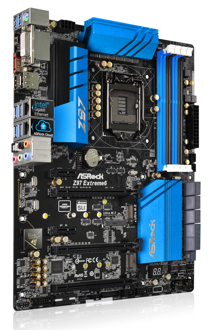
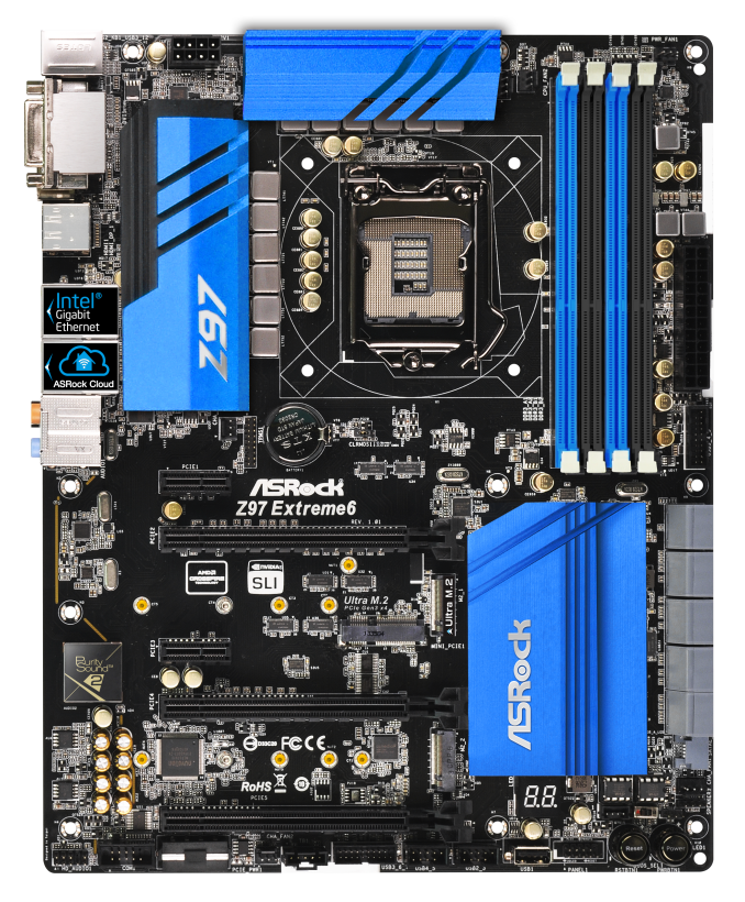
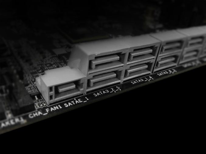
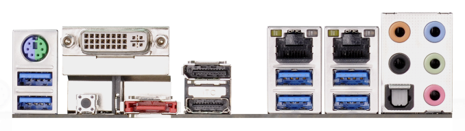


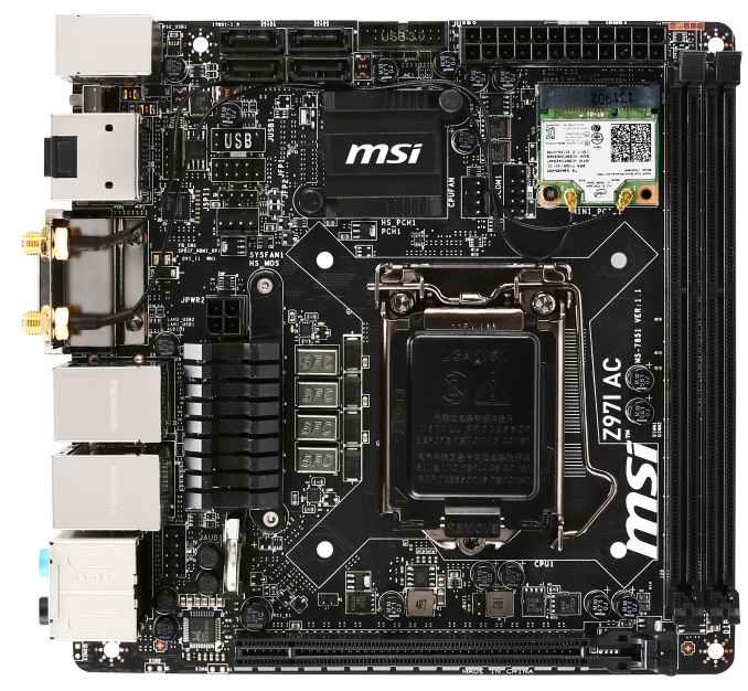


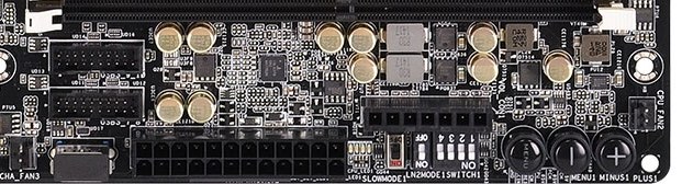


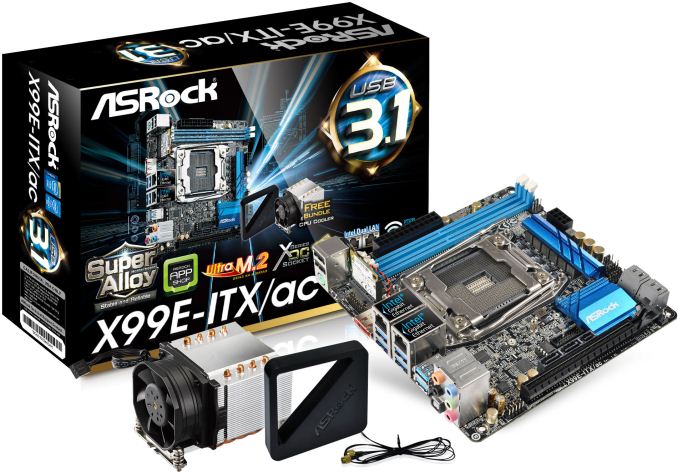
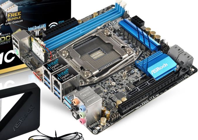
_678x452.jpg)

